Surface treatment of inter-layer dielectric

a surface treatment and dielectric technology, applied in the direction of semiconductor devices, semiconductor/solid-state device details, electrical apparatus, etc., can solve the problems of metal contact performance degradation and shortage of semiconductor devices

Inactive Publication Date: 2007-09-27
GLOBALFOUNDRIES INC
View PDF22 Cites 43 Cited by
  • Summary
  • Abstract
  • Description
  • Claims
  • Application Information

AI Technical Summary

Benefits of technology

[0015] According to one embodiment of the invention, the size of a typical gas cluster used in the GCIB process may be around, e.g., 5 nm, which is bigger than the size of a typical pore, which is around, e.g., 1˜2 nm, inside a porous ULK material. Therefore, surface treatment by a GCIB process may not cause changes in the property of the bulk ULK material. In the mean time, the GCIB surface treatment may create a smooth layer of densified surface in the ULK dielectric material. According to one embodiment of the invention, the thickness of a densified layer may be controlled preferably by an acceleration voltage used in the GCIB process. According to another embodiment, the thickness of a densified layer may be from 10 Å to 5000 Å, and may be preferably in the range of 50 Å-250 Å.
[0016] Af

Problems solved by technology

This penetration or intrusion of metal element into porous ULK ILD may cause performance degradation of the metal contacts f

Method used


Image

  • Surface treatment of inter-layer dielectric
  • Surface treatment of inter-layer dielectric
  • Surface treatment of inter-layer dielectric

Examples


Embodiment Construction

[0031] As is known in the art, manufacture of a semiconductor device may include processing of, for example, a front end of line (FEOL) and a back end of line (BEOL). During a FEOL processing, semiconductor devices such as, for example, switches and logic gates may be produced. These devices may be interconnected through one or more interconnect structures. The interconnect structures may be produced through a BEOL processing.

[0032] A conventional BEOL processing may include steps such as, for example, cap deposition, ILD deposition, hard mask or photo-mask deposition, lithography, and etching, among other steps. For the interest of not obscuring the presentation of the essences of present invention, processing steps that are well known in the art may not be described below in detail, but rather the following description will focus on the distinctive elements of the present invention.

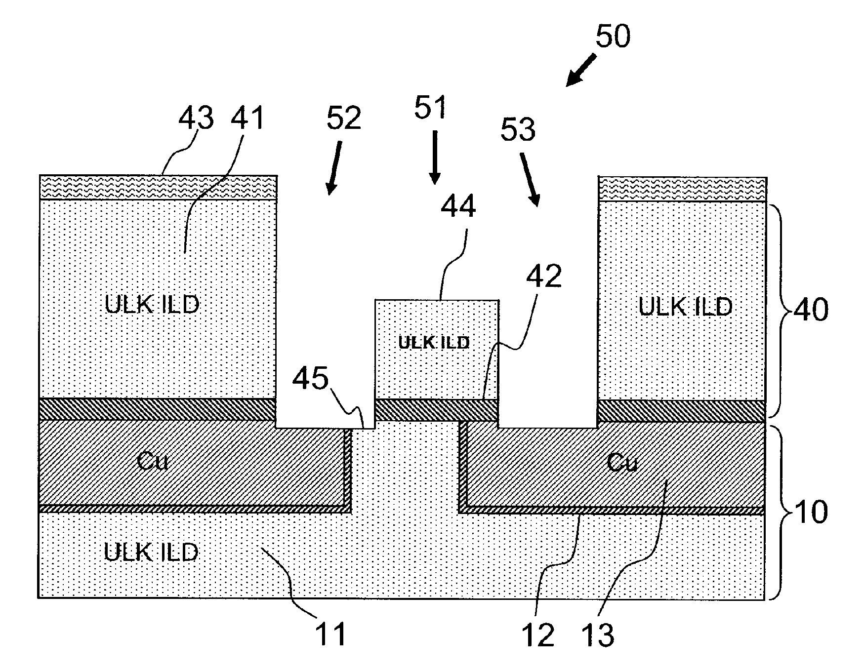
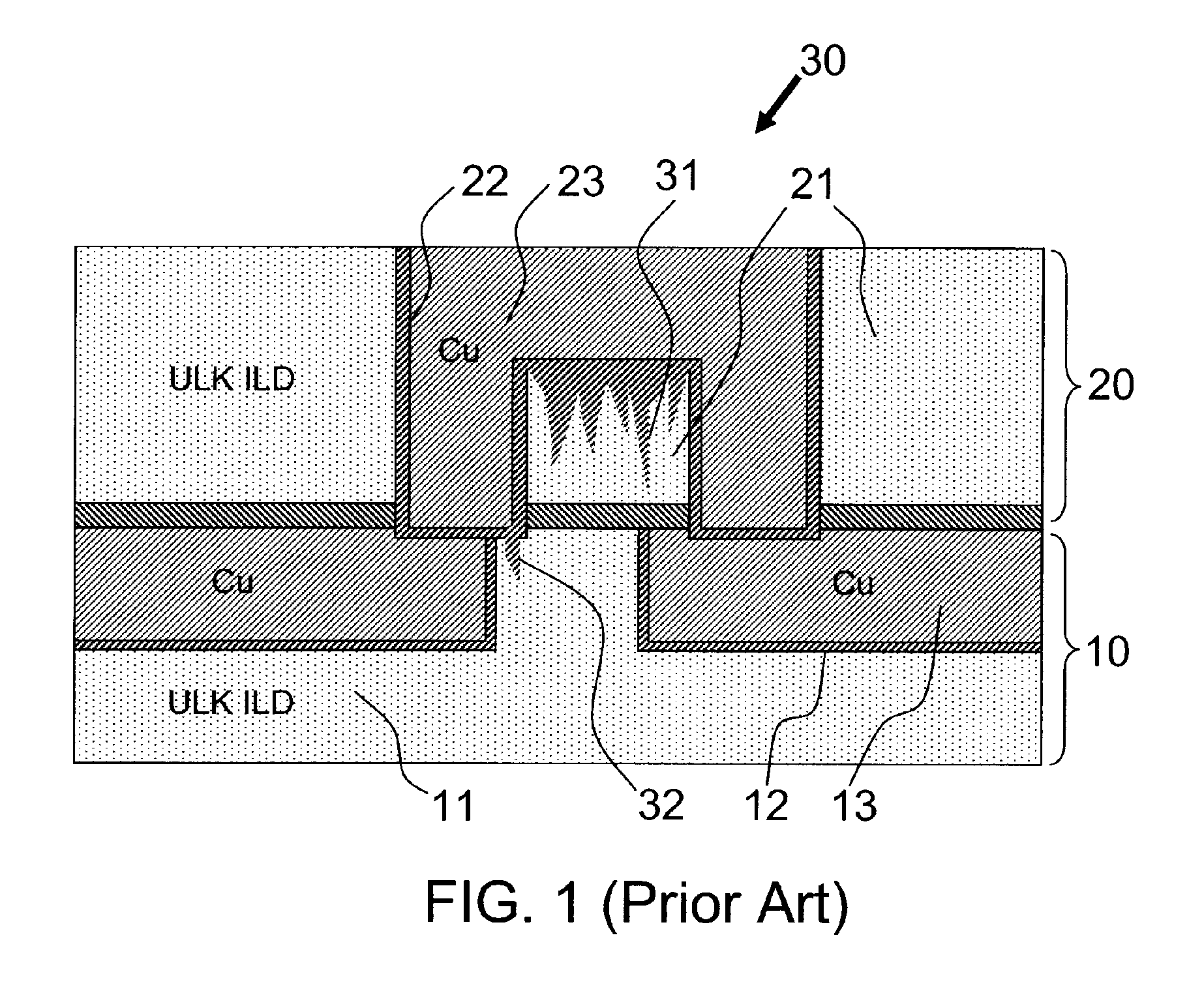
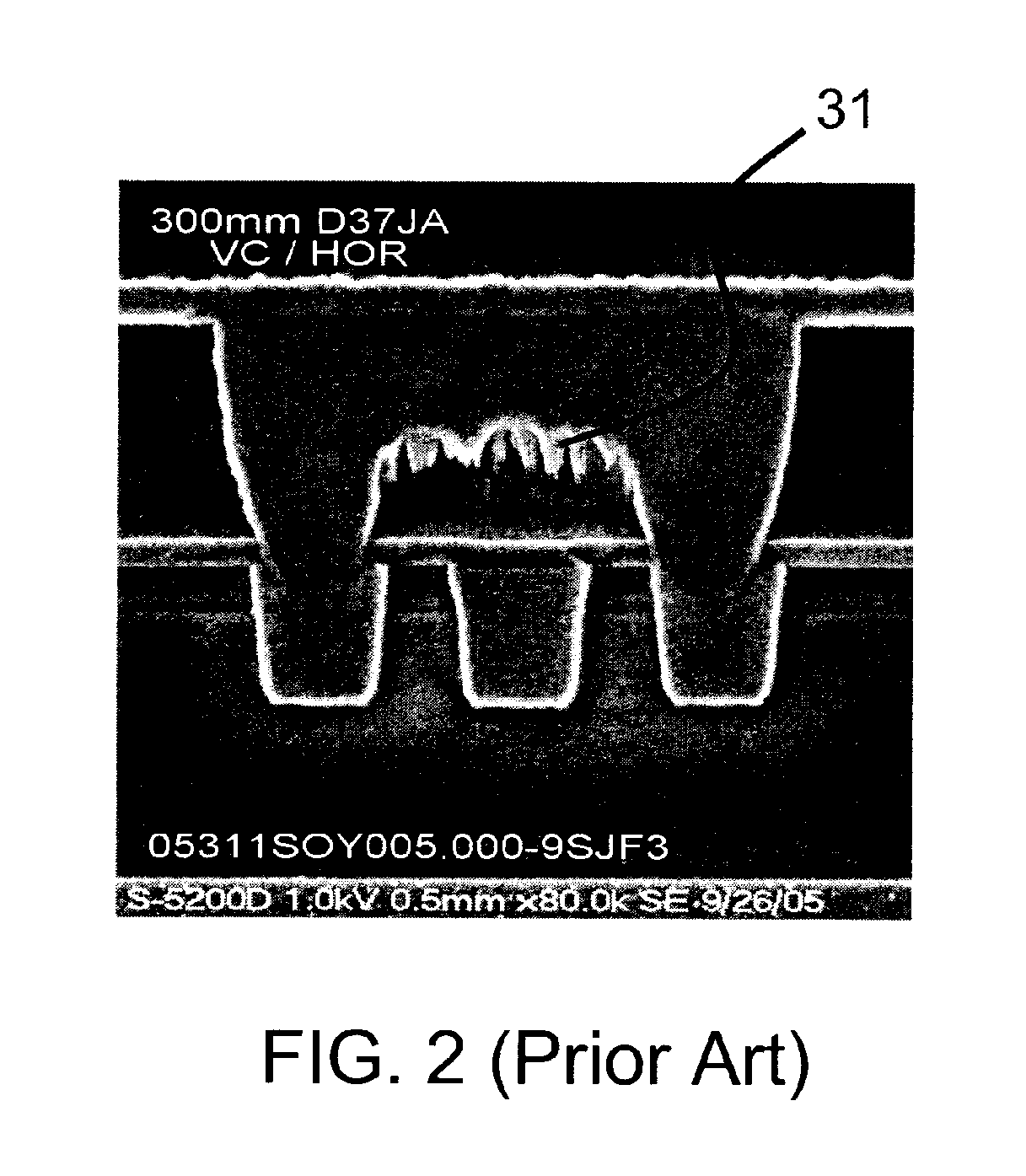
[0033]FIG. 1 is a schematic illustration of an interconnect structure as is known in the art. Inte...


PUM


Abstract

When an interconnect structure is built on porous ultra low k (ULK) material, the bottom of the trench and/or via is usually damaged by a following metallization process which may be suitable for dense higher dielectric materials. Embodiment of the present invention may provide a method of forming an interconnect structure on an inter-layer dielectric (ILD) material. The method includes steps of treating an exposed area of said ILD material to create a densified area, and metallizing said densified area.

Description

FIELD OF THE INVENTION [0001] The current invention relates to the field of semiconductor device manufacturing. In particular, it relates to a process of providing treatment to surfaces of an interconnect structure after etching and before metallization. BACKGROUND OF THE INVENTION [0002] Recent rapid advancement in semiconductor technology has brought the advent of very large scale integrated (VLSI) as well as ultra large scale integrated (ULSI) circuitries, resulting in integration of more devices into smaller areas on a single semiconductor substrate. In order to further enhance performance of the VLSI and / or ULSI circuitries, ultra-low dielectric constant (ULK) materials, such as porous materials, are being used as inter-layer dielectric (ILD) to further reduce capacitance such as, for example, inter-layer capacitance and / or other parasitic capacitance that may be undesirable to the performance such as speed of the VLSI and / or ULSI circuitries. Interconnect structures made of me...

Claims


Application Information

Patent Timeline
IPC IPC(8): H01L23/52
CPCH01L21/3105H01L21/76825H01L21/76808H01L21/31058H01L21/76814H01L21/76831
Inventor CHEN, SHYNG-TSONGLIN, QINGHUNGMALONE, KELLYMEHTA, SANJAYSPOONER, TERRY A.YANG, CHIH-CHAO
Owner GLOBALFOUNDRIES INC
Why Eureka
Try Eureka