Semiconductor integrated circuit and semiconductor integrated circuit device

a technology of integrated circuits and semiconductors, applied in the direction of dc-dc conversion, digital data processing details, instruments, etc., can solve the problems of data loss, difficult to arrange the entire multiplex power supply circuit on the semiconductor chip (lsi), and the semiconductor chip stops operating, etc., to improve the reliability of the semiconductor integrated circuit device

Inactive Publication Date: 2007-09-27
GOOGLE LLC
View PDF6 Cites 24 Cited by
  • Summary
  • Abstract
  • Description
  • Claims
  • Application Information

AI Technical Summary

Benefits of technology

[0006] Thereupon, an advantage of this invention is to improve the reliability of a semiconductor integrated circuit device by enabling power to be fed to a semiconductor chip even upon a partial failure in its power supply.
[0008] In the foregoing semiconductor integrated circuit, because the power supply circuit for supplying power to the semiconductor chip is multiplexed, even when a failure occurs in one of the power supplies, a different normally-operating power supply can supply power to the semiconductor chip, thereby improving the reliability of the LSI chip is improved.
[0010] According to this invention, the power can be supplied to the semiconductor chip even upon a partial failure in its power supply circuit, thereby improving the reliability of the semiconductor integrated circuit device.

Problems solved by technology

However, because the power supply circuit is not multiplexed, once the power supply circuit has a problem, the semiconductor chip stops operating.
In disk array system having semiconductor chips mounted therein, when the semiconductor chips stop operating due to power failures in their power supply circuits, data may be lost.
However, with a semiconductor chip (LSI) requiring considerable power, the size of its power supply circuit is large, therefore, it is difficult to arrange the entire multiplex power supply circuit on the semiconductor chip (LSI).
Also, even if the entire multiplex power supply circuit can be mounted on one semiconductor chip, when a failure occurs in the power supply circuit, the semiconductor chip itself has to be replaced, which raises the cost of recovering from the failure.
Considering that power supply circuits are relatively cheaper than semiconductor chips, it is not desirable to replace the semiconductor chips when failures occur in the power supply circuits.

Method used


Image

  • Semiconductor integrated circuit and semiconductor integrated circuit device
  • Semiconductor integrated circuit and semiconductor integrated circuit device
  • Semiconductor integrated circuit and semiconductor integrated circuit device

Examples


example 2

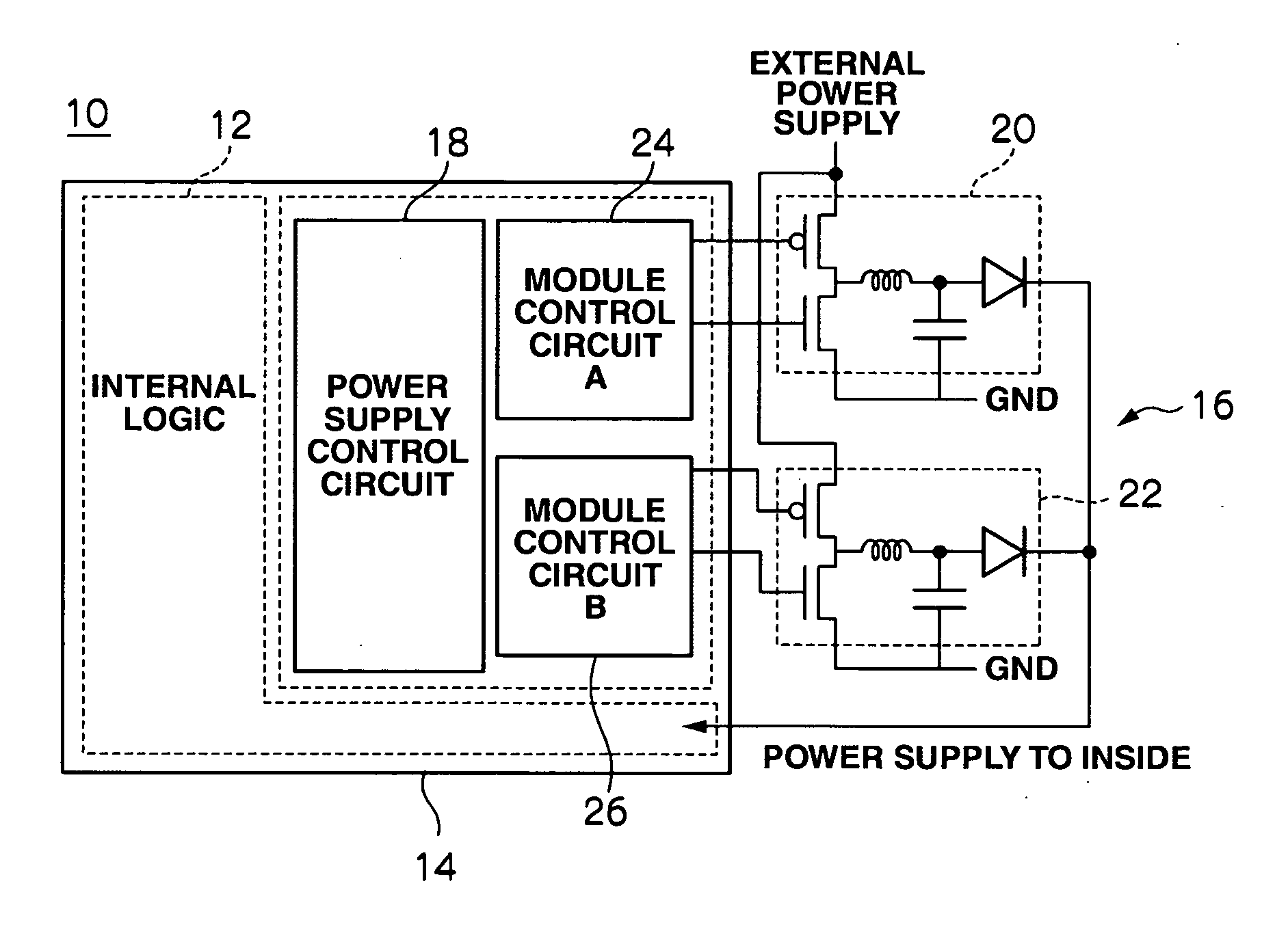
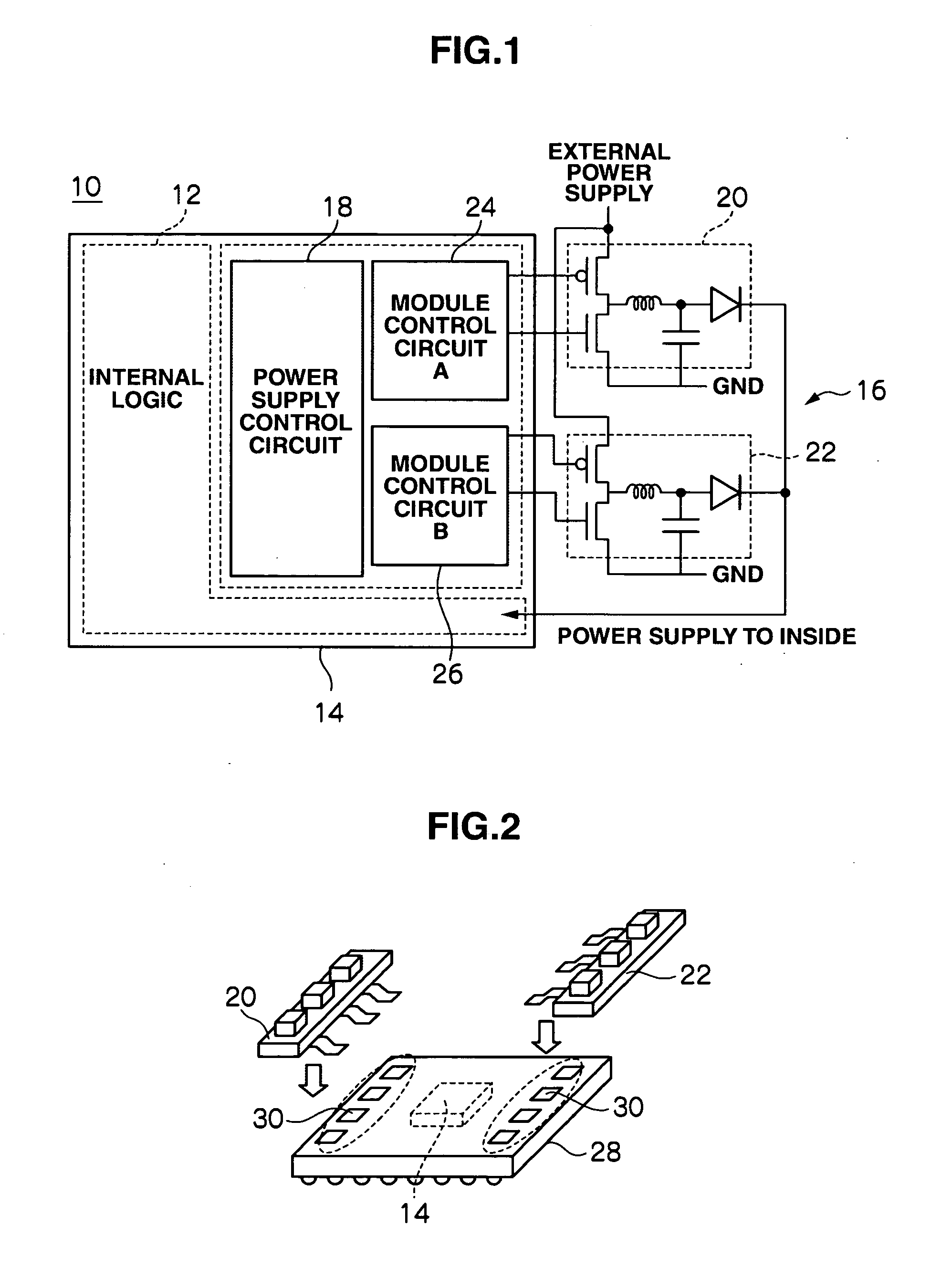
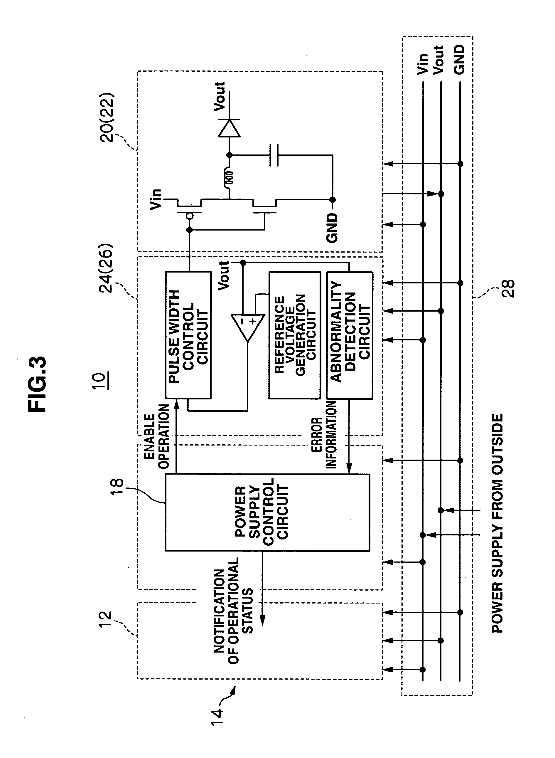
[0052] Example 2 of this invention will be explained with reference to FIGS. 4 and 5. In this example, LSI chips (semiconductor chips) 14 and 15 and an external microcomputer 52 are mounted on a single substrate 50 and information is transmitted between the LSI chips 14 and 15 and the microcomputer 52 using signals such as operation status control signals 200 and 202, internal logic reset signals 204 and 206, and power supply control circuit reset signals 208 and 210. Power supply circuits 16 and 17 are each multiplexed, i.e., there are power supply circuits 16A, 16B and power supply circuits 17A, 17B. The power supply circuit 16A has an external module 20A and module control circuit 24A; the power supply circuit 16B has an external module 20B and module control circuit 24B; the power supply circuit 17A has an external module 22A and module control circuit 26A; and the power supply circuit 17B has an external module 22B and module control circuit 26B. The LSI chips 14 and 15 have in...


PUM


Abstract

An LSI chip has an internal logic, power supply control circuit and module control circuits, mounted thereon. External modules are provided outside the LSI chip. A power supply circuit for supplying power to the internal logic is composed of the module control circuits and external modules, that is, the power supply circuit is multiplexed, so that if a failure occurs in one of the power supplies, a different normally-operating power supply supplies power to the internal logic. Accordingly, the reliability of the LSI chip is improved.

Description

CROSS REFERENCES TO RELATED APPLICATIONS [0001] This application relates to and claims priority from Japanese Patent Application No. 2006-083837, filed on Mar. 24, 2006 the entire disclosure of which is incorporated herein by reference. BACKGROUND OF THIS INVENTION [0002] The present invention relates to a semiconductor integrated circuit with a built-in power supply circuit for stepping down the voltage of an external power supply; and a semiconductor integrated circuit device. For example, this invention relates to a technique suitable for use in storage systems having disk array apparatuses that require low-voltage and low-power semiconductor chips. [0003] In accordance with the trend toward low operating voltages in semiconductor chips with logic circuits (internal logic), e.g., large scale integrated circuit (LSI) chips, semiconductor chips (LSI chips) with built-in power supply circuits such as DC-DC converters have been known. With the power supply circuits included in the se...

Claims


Application Information

Patent Timeline
Patent Type & Authority Applications(United States)
IPC IPC(8): G01R31/28
CPCG01R31/31721H02M3/1584G11C5/147
Inventor FUSEYA, TOMOKATSU
Owner GOOGLE LLC
Why Eureka
Try Eureka