Electronic circuit and integrated circuit including scan testing circuit, and power consumption reducing method used for integrated circuit

a technology of integrated circuits and scan testing circuits, applied in electronic circuit testing, measurement devices, instruments, etc., can solve the problems of power consumption waste, conventional techniques, and technique not suiting the needs and achieve the effect of reducing power consumption in normal operation mod

Inactive Publication Date: 2007-09-27
NEC CORP
View PDF6 Cites 16 Cited by
  • Summary
  • Abstract
  • Description
  • Claims
  • Application Information

AI Technical Summary

Benefits of technology

[0017]In an integrated circuit including scan flip-flops and a scan testing capability according to the present invention, a power-supply controller applies a power-supply voltage to internal and external transmission circuits in scan test mode and stops applying the power supply voltage in normal operation mode. Thus, power consumption associated with operations of the internal and external transmission circuits is eliminated, thereby reducing power consumption in normal operation mode.
[0018]A signal transmission stopping device stops transmission of a signal through the internal and external circuits in normal operation mode. This prevents power consumption associated with signal transmission, thus reducing power consumption in normal operation mode.

Problems solved by technology

However, there is a problem with LSIs including a scan testing circuit that the scan testing circuit also operates during normal operation and thus wastes power.
However, these conventional techniques have the following problems.
Because of the same reason, the technique does not suite for reducing power consumption of flip-flop with scan testing circuit.

Method used


Image

  • Electronic circuit and integrated circuit including scan testing circuit, and power consumption reducing method used for integrated circuit
  • Electronic circuit and integrated circuit including scan testing circuit, and power consumption reducing method used for integrated circuit
  • Electronic circuit and integrated circuit including scan testing circuit, and power consumption reducing method used for integrated circuit

Examples


Embodiment Construction

:

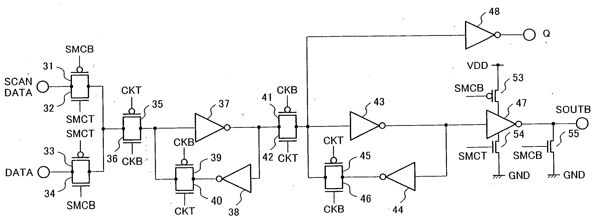
[0027]FIGS. 1A to 1C are a circuit diagram illustrating an exemplary embodiment of the present invention. The LSI illustrated in FIGS. 1A to 1C are an integrated circuit including a scan testing circuit. FIG. 1A shows the main portion of one of scan-chained FFs. The circuit shown in FIG. 1A includes a pMOS 31, nMOS 32, pMOS 33, nMOS 34, pMOS 35, nMOS 36, inverters 37 and 38, a pMOS 39, nMOS 40, pMOS 41, nMOS 42, inverters 43 and 44, pMOS 45, nMOS 46, inverters 47 and 48, pMOS 53, and nMOSs 54 and 55. FIG. 1B shows a circuit which consists of inverters 49 and 50 and relates to a CLK signal. FIG. 1C shows a circuit which consists of inverters 51 and 52 and relates to a SCANMODE signal. The elements shown in FIGS. 1A to 1C constitute an FF. The LSI also includes multiple scan-chained FFs, not shown, each having the same configuration that is described above.

[0028]The pMOS 31 is turned on and off by a control signal SMCB which is a mode setting signal SCANMODE inverted by the inverter ...


PUM


Abstract

An integrated circuit with a scan testing circuit which enables reducing power consumption in normal operation mode is provided. A power-supply controller applies a power-supply voltage to internal and external transmission circuits in scan test mode and stops applying the power supply voltage in normal operation mode. Thus, power consumption associated with operations of the internal and external transmission circuits is eliminated, thereby reducing power consumption in normal operation mode.

Description

BACKGROUND OF THE INVENTION[0001]1. Field of the Invention[0002]The present invention relates to an electronic circuit and an integrated circuit including a scan testing circuit, and a power consumption reducing method used for the integrated circuit and, in particular, to an electronic circuit and an integrated circuit including a scan testing circuit that are capable of reducing power consumption in normal operation mode other than in scan testing mode, and a power consumption reducing method used for the integrated circuit.[0003]2. Description of the Related Art[0004]LSIs (Large Sale Integrated circuits) comprising multiple flip-flops (FFs) also have an embedded circuit for a scan being carried out as an operation test of the LSIs at manufacturing time. These LSIs are called scan-testable integrated circuits. In scan-based testing, each of the FFs of the LSI enters scan test mode in which the FFs are chained together into a shift register called a scan chain. A test input signal ...

Claims


Application Information

Patent Timeline
Patent Type & Authority Applications(United States)
IPC IPC(8): G01R31/28
CPCG01R31/318575G01R31/318536
Inventor UCHIDA, KOHEY
Owner NEC CORP
Why Eureka
Try Eureka