Interconnect structure having a silicide/germanide cap layer

a technology of silicide and germanide, applied in the direction of semiconductor devices, semiconductor/solid-state device details, electrical apparatus, etc., can solve the problems of increasing the probability of via failure, increasing the density, and still suffering from reliability issues of copper electro migration (em) and stress migration (sm), so as to improve the overall resistance and reliability of the interconnect structure.

Inactive Publication Date: 2007-10-04
TAIWAN SEMICON MFG CO LTD
View PDF5 Cites 30 Cited by
  • Summary
  • Abstract
  • Description
  • Claims
  • Application Information

AI Technical Summary

Benefits of technology

[0015]With the silicide / germanide layers formed on top of the copper lines, the overall resistance and reliability of the interconnect structure are improved.

Problems solved by technology

However, copper still suffers from electro migration (EM) and stress migration (SM) reliability issues as geometries continue to shrink and current densities increase.
However, the introduction of cap layer 16 generates another problem.
A more severe problem is that the probability of via failure increases.

Method used


Image

  • Interconnect structure having a silicide/germanide cap layer
  • Interconnect structure having a silicide/germanide cap layer
  • Interconnect structure having a silicide/germanide cap layer

Examples


Embodiment Construction

[0022]The making and using of the presently preferred embodiments are discussed in detail below. It should be appreciated, however, that the present invention provides many applicable inventive concepts that can be embodied in a wide variety of specific contexts. The specific embodiments discussed are merely illustrative of specific ways to make and use the invention, and do not limit the scope of the invention.

[0023]A novel interconnect structure for integrated circuits and a method of forming the same are provided. The intermediate stages of manufacturing a preferred embodiment of the present invention are illustrated. The variations of the preferred embodiments are discussed. Throughout the various views and illustrative embodiments of the present invention, like reference numbers are used to designate like elements.

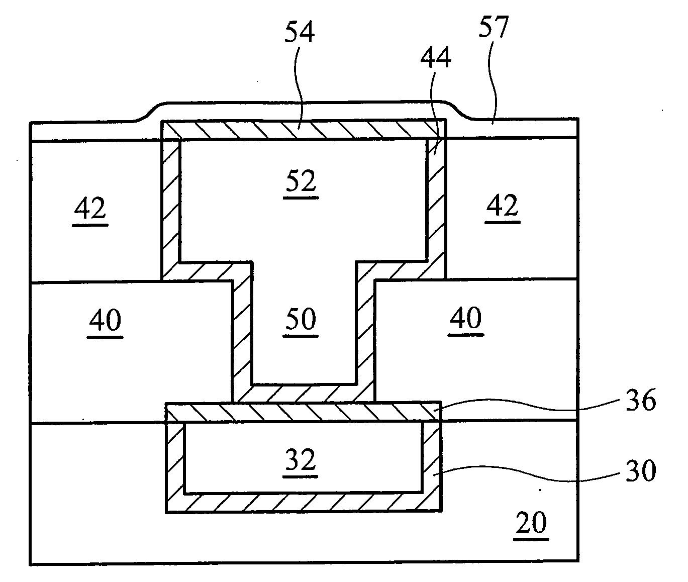
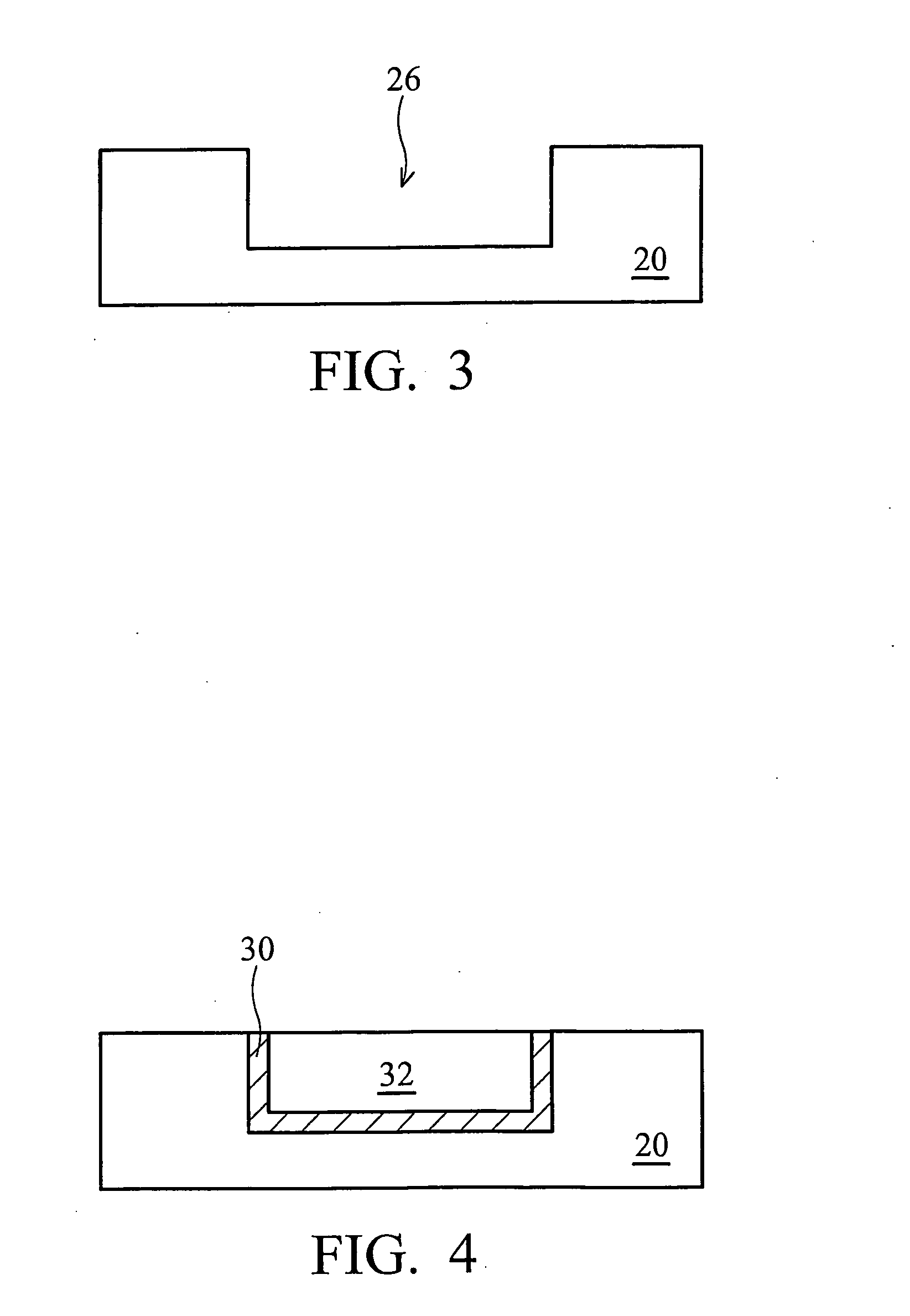
[0024]FIGS. 3 through 8 are cross-sectional views of intermediate stages in the making of a preferred embodiment of the present invention. FIG. 3 illustrates the form...


PUM


Abstract

An interconnect structure of an integrated circuit and a method for forming the same are provided. The interconnect structure includes a semiconductor substrate, a low-k dielectric layer over the semiconductor substrate, a conductor in the low-k dielectric layer, and a cap layer on the conductor. The cap layer has at least a top portion comprising a metal silicide / germanide.

Description

[0001]This application claims the benefit of U.S. Provisional Application No. 60 / 789,028, filed on Apr. 4, 2006, entitled “Interconnect Structure Having a Silicide / Germanide Cap Layer,” which application is hereby incorporated herein by reference.TECHNICAL FIELD[0002]This invention is related generally to integrated circuits, and more particularly to the structure and methods of interconnect structures in integrated circuits.BACKGROUND[0003]A conventional integrated circuit contains a plurality of patterns of metal lines separated by inter-wiring spacings and a plurality of interconnect lines, such as bus lines, bit lines, word lines and logic interconnect lines. Typically, the metal patterns of vertically spaced metallization layers are electrically interconnected by vias. Metal lines formed in trench-like openings typically extend substantially parallel to the semiconductor substrate. Semiconductor devices of such type, according to current technology, may comprise eight or more l...

Claims


Application Information

Patent Timeline
Patent Type & Authority Applications(United States)
IPC IPC(8): H01L23/52
CPCH01L21/76826H01L21/76829H01L21/76834H01L21/76849H01L21/76856H01L21/76864H01L2924/0002H01L23/53238H01L23/5329H01L2924/00
Inventor YU, CHEN-HUALU, YUNG-CHENGCHANG, HUI-LIN
Owner TAIWAN SEMICON MFG CO LTD
Why Eureka
Try Eureka