Field emission backlight, display apparatus using the same and a method of manufacturing the same

a field emission backlight and display apparatus technology, applied in the direction of discharge tube/lamp details, discharge tube luminescnet screen, instruments, etc., can solve the problems of increasing the cost of the driving circuit of the triode field emission backlight incorporating such a structure, and the electrical power consumption is large, so as to reduce the cost

Inactive Publication Date: 2007-10-04
SAMSUNG DISPLAY CO LTD
View PDF0 Cites 8 Cited by
  • Summary
  • Abstract
  • Description
  • Claims
  • Application Information

AI Technical Summary

Benefits of technology

[0008] In accordance with the exemplary embodiments thereof described herein, the present invention provides field emission backlights for display devices and methods for manufacturing them at a s

Problems solved by technology

However, one of the problems with conventional field emission backlights is that they consume a large amount of electrical power because of the high voltage that needs to be applied between the transparent electrode and the electrode part.
However, the cost

Method used


Image

  • Field emission backlight, display apparatus using the same and a method of manufacturing the same
  • Field emission backlight, display apparatus using the same and a method of manufacturing the same
  • Field emission backlight, display apparatus using the same and a method of manufacturing the same

Examples


Embodiment Construction

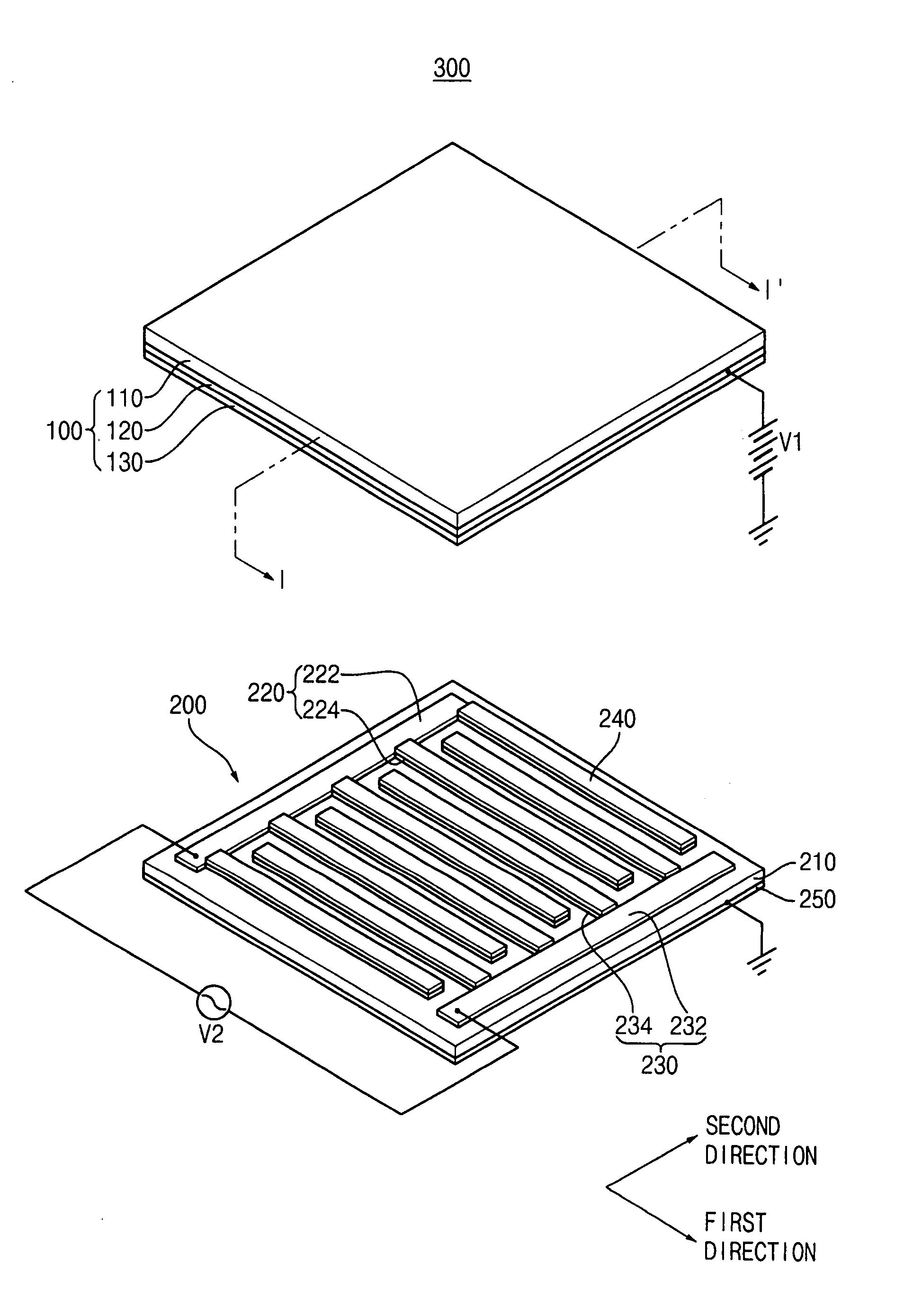
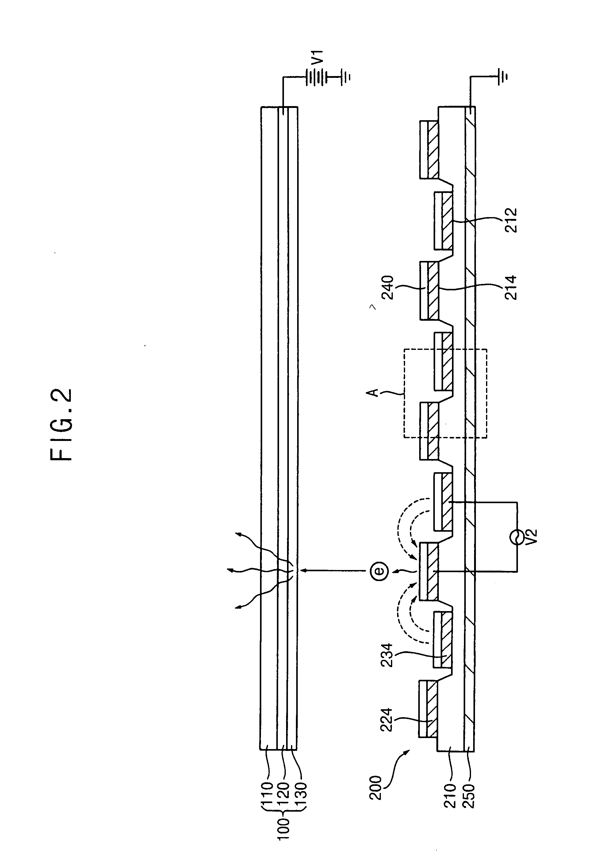
[0023]FIG. 1 is an exploded perspective view of an exemplary embodiment of a field emission backlight for a display apparatus in accordance with the present invention, and FIG. 2 is a partial cross-sectional view of the exemplary backlight as seen along the lines of the section I-I′ taken in FIG. 1;

[0024] Referring to FIGS. 1 and 2, a field emission backlight 300 includes an upper substrate 100 and a lower substrate 200. The field emission backlight 300 generates light through an electric field applied between the upper substrate 100 and the lower substrate 200. The generated light exits upwardly from the field emission backlight 100.

[0025] The upper substrate 100 includes an upper transparent substrate 110, a transparent electrode 120 and a fluorescent part 130. The upper transparent substrate 110 is plate shaped and comprises a transparent material, for example, glass, quartz or a transparent plastic. Preferably, the upper transparent substrate 110 comprises glass.

[0026] The tr...


PUM


Abstract

A field emission backlight for a display device includes upper and lower substrates. The upper substrate includes an upper transparent substrate, a transparent electrode, and a fluorescent part. The lower substrate includes a lower transparent substrate having a receiving groove, a first electrode part, a second electrode part, and an electron-emitting part. The first electrode part is formed on an upper surface of the lower transparent substrate and the second electrode part is formed on a bottom surface of the receiving groove, so that the gap between the first and second electrode parts can be reduced below that conventionally required. This, in turn, enables the level of a voltage applied between the first and the second electrode parts to be reduced, and a corresponding reduction in the manufacturing cost of a field emission backlight to be achieved.

Description

RELATED APPLICATIONS [0001] This application claims priority of Korean Patent Application No. 2006-20256, filed Mar. 3, 2006, the entire disclosure of which is incorporated herein by reference. BACKGROUND [0002] This disclosure relates to making field emission backlights for display devices, such as liquid crystal displays (LCDs), and more particularly, to methods for making field emission backlights that substantially reduce their manufacturing costs. [0003] Liquid crystal displays (LCDs) generally include an LCD panel that displays an image by using the optical transmittance of a layer of liquid crystal material disposed in the panel and the light produced by a backlight assembly disposed behind the panel. [0004] Backlight assemblies can be classified according to the type of light sources used therein, e.g., cold cathode fluorescent lamp (CCFL) backlights, external electrode fluorescent lamp (EEFL) backlights, light emitting diode (LED) backlights, and so on. [0005] A recent inno...

Claims


Application Information

Patent Timeline
IPC IPC(8): H01J1/62H01J63/04
CPCG02F1/133602G02F2001/133625H01J63/06H01J63/02H01J63/04H01J61/305G02F1/133625H05B33/10H05B33/22H05B33/26
Inventor YOO, HYEONG-SUKJOO, SEUNG-KI
Owner SAMSUNG DISPLAY CO LTD
Why Eureka
Try Eureka