Apparatus and method for processing substrates using one or more vacuum transfer chamber units

a vacuum transfer chamber and apparatus technology, applied in conveyor parts, transportation and packaging, coatings, etc., can solve the problems of increasing exposing the substrate to potential contamination, and reducing so as to reduce the overall processing time, and the overall processing time. , to achieve the effect of reducing the cost of ownership to end users, reducing the complexity and manufacturing cost of the apparatus

a vacuum transfer chamber and apparatus technology, applied in conveyor parts, transportation and packaging, coatings, etc., can solve the problems of increasing exposing the substrate to potential contamination, and reducing so as to reduce the overall processing time, and the overall processing time. , to achieve the effect of reducing the cost of ownership to end users, reducing the complexity and manufacturing cost of the apparatus

US20070231109A1Inactive Publication Date: 2007-10-04ARCUS TECH

Image

  • Apparatus and method for processing substrates using one or more vacuum transfer chamber units
  • Apparatus and method for processing substrates using one or more vacuum transfer chamber units
  • Apparatus and method for processing substrates using one or more vacuum transfer chamber units

Examples


Embodiment Construction

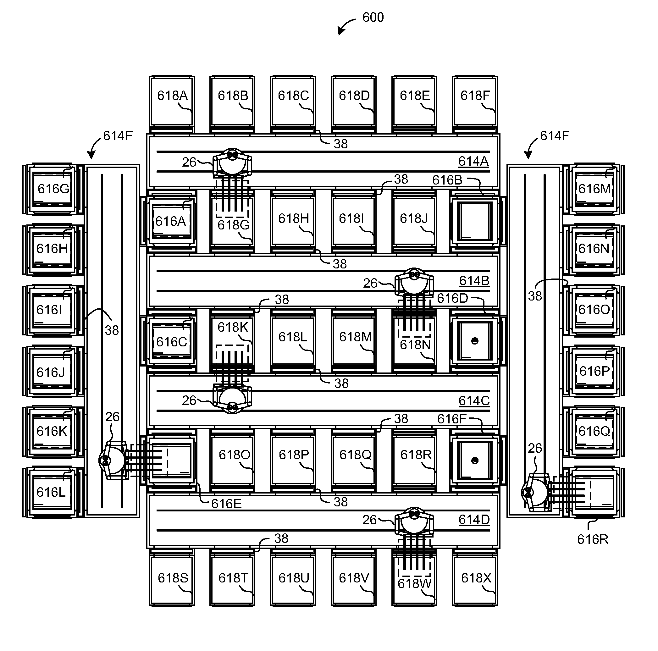
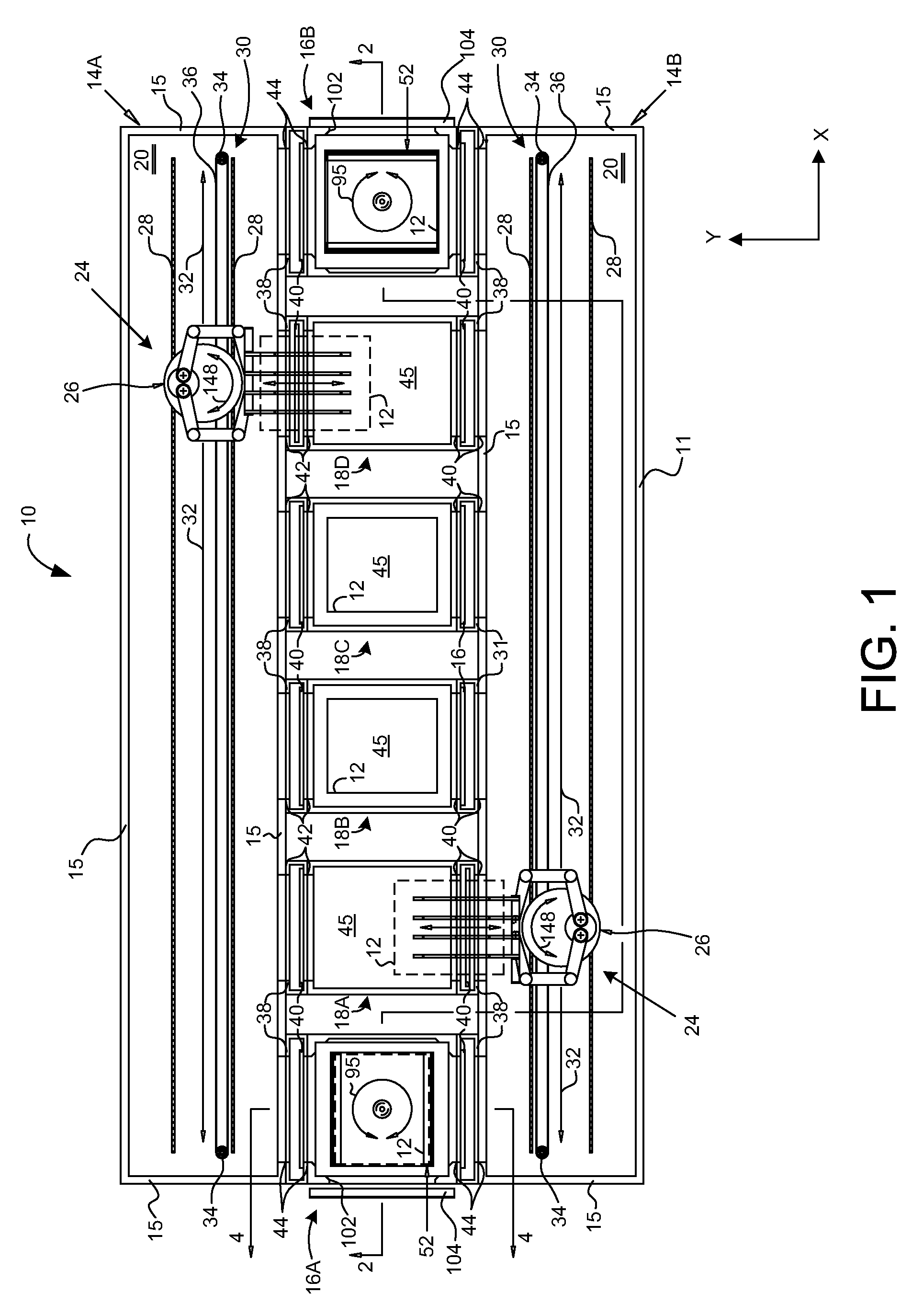
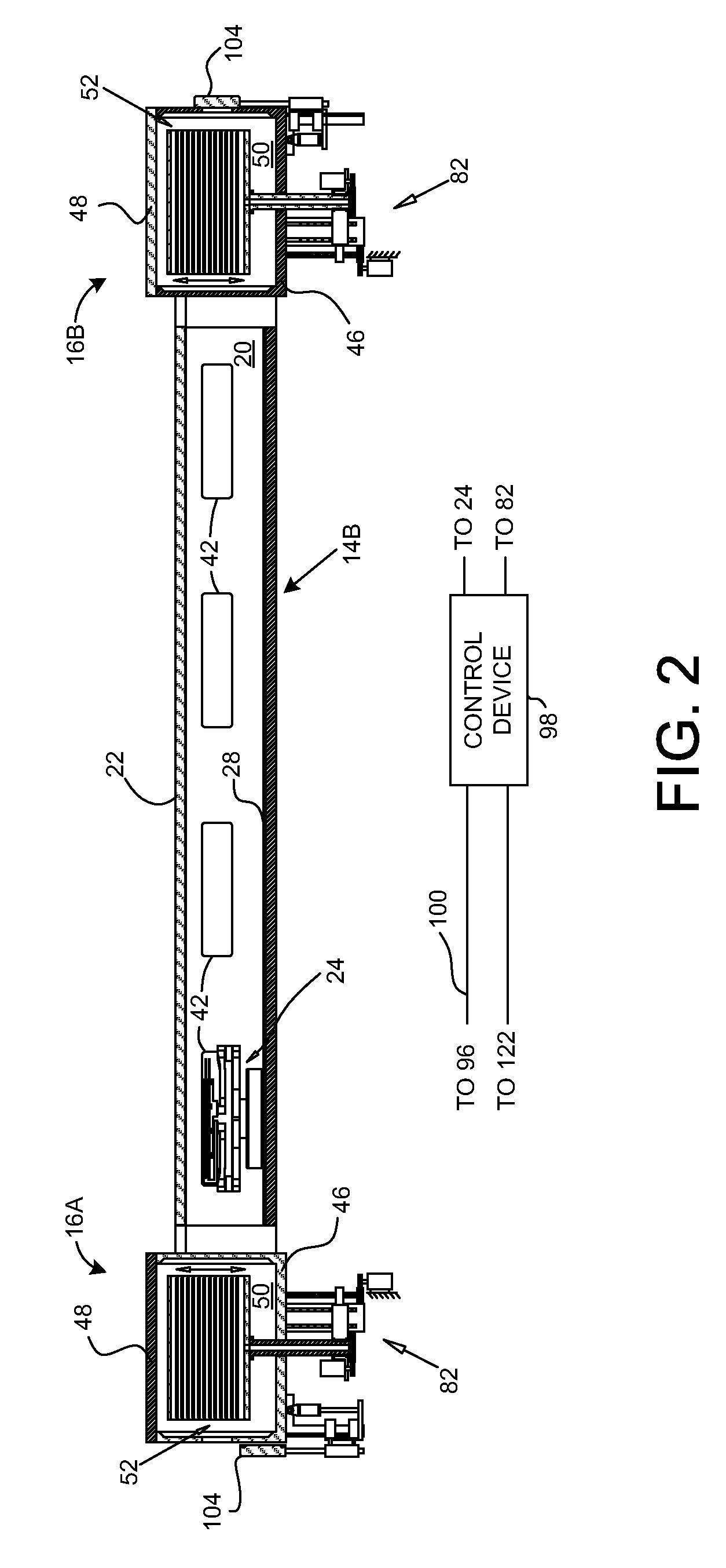
[0024]With reference to FIG. 1, an apparatus 10 for processing substrates 12, such as semiconductor and flat panel display substrates, in accordance with an embodiment of the invention is described. FIG. 1 is a top plan view of the apparatus 10, which is shown with top lids removed. FIG. 2 is a vertical cross-sectional view, partly schematic, of the apparatus 10 along line 2-2 in FIG. 1. The apparatus 10 is an integrated modular multiple chamber vacuum processing system. The apparatus 10 includes one or more vacuum transfer chamber units 14A and 14B, one or more load lock chamber units 16A and 16B, and one or more vacuum process chamber units 18A, 18B, 18C and 18D. Each of the vacuum process chamber units 18A, 18B, 18C and 18D is configured to perform a specific semiconductor integrated circuit (IC) or flat panel display (FPD) fabrication process, such as gas chemistry high density plasma etching, plasma enhanced gas chemistry deposition, atomic layer deposition, physical vapor depo...


PUM

PropertyMeasurementUnit
Densityaaaaaaaaaa
Vacuumaaaaaaaaaa

Abstract

An apparatus and method for processing substrates uses one or more vacuum transfer chamber units to transfer some of the substrates between at least one load lock chamber unit and at least one vacuum process chamber unit.

Description

CROSS REFERENCE TO RELATED APPLICATION[0001]This application is entitled to the benefit of U.S. Provisional Patent Application Ser. No. 60 / 787,079 filed on Mar. 28, 2006, which is incorporated herein by reference.BACKGROUND OF THE INVENTION[0002]Fabrication of semiconductor integrated circuits and flat panel displays involves numerous processes, such as etching, chemical vapor deposition, sputtering and cleaning, which are performed on semiconductor and flat panel display substrates. Each of these processes may be performed using a different single processing tool, i.e., a tool that performs a single fabrication process. Since multiple fabrication processes must be performed, the substrates must be transferred from one processing tool to the next, which exposes the substrates to potential contamination. In addition, transferring substrates between different processing tools increases the overall processing time.[0003]Consequently, multiple processing tools have been developed that c...

Claims


Application Information

Patent Timeline
04 Oct 2007
Publication
US20070231109A1
IPC
H01L21/677
CPC
C23C16/54; H01L21/67126; H01L21/67236; H01L21/67184; H01L21/67173
Inventors
PAK, SAMUEL S.; CHANG, CHRISTOPHER C.