Light emitting diode package having anodized insulation layer and fabrication method therefor

a technology of light-emitting diodes and anodized insulation, which is applied in the direction of semiconductor devices, electrical devices, semiconductor/solid-state device details, etc., can solve the problems of increasing assembly costs, hindering a simplified manufacturing process, and ineffective heat radiation during light-emitting operation, so as to improve the lifetime and light-emitting efficiency of leds, and superior heat radiation effect of leds through substrates

Active Publication Date: 2007-10-11
SAMSUNG ELECTRONICS CO LTD
View PDF8 Cites 46 Cited by
  • Summary
  • Abstract
  • Description
  • Claims
  • Application Information

AI Technical Summary

Benefits of technology

[0011]The present invention has been made to solve the foregoing problems of the prior art and therefore an aspect of the present invention is to provide an LED package having an anodized insulation layer, which has a superior heat radiation effect of an LED through a substrate, thereby increasing the lifetime and light emission efficiency of the LED, and a fabrication method therefor.

Problems solved by technology

However, in the conventional LED package 200, the substrate 210 is not made of a material with high heat conductivity, i.e., good heat radiation capacity, for example, aluminum (Al), and thus heat radiation is not effective during the light emission operation of the LED 215.
In addition, the conventional LED package 200 needs to have the reflecting member 220 fixed by a separate process, hindering a simplified manufacturing processes.
Furthermore, the rather inaccurate process of integrating the reflecting member 220 with the substrate can be a major cause of defective products, thereby increasing the assembly costs.

Method used


Image

  • Light emitting diode package having anodized insulation layer and fabrication method therefor
  • Light emitting diode package having anodized insulation layer and fabrication method therefor
  • Light emitting diode package having anodized insulation layer and fabrication method therefor

Examples


Embodiment Construction

[0032]Exemplary embodiments of the present invention will now be described in detail with reference to the accompanying drawings.

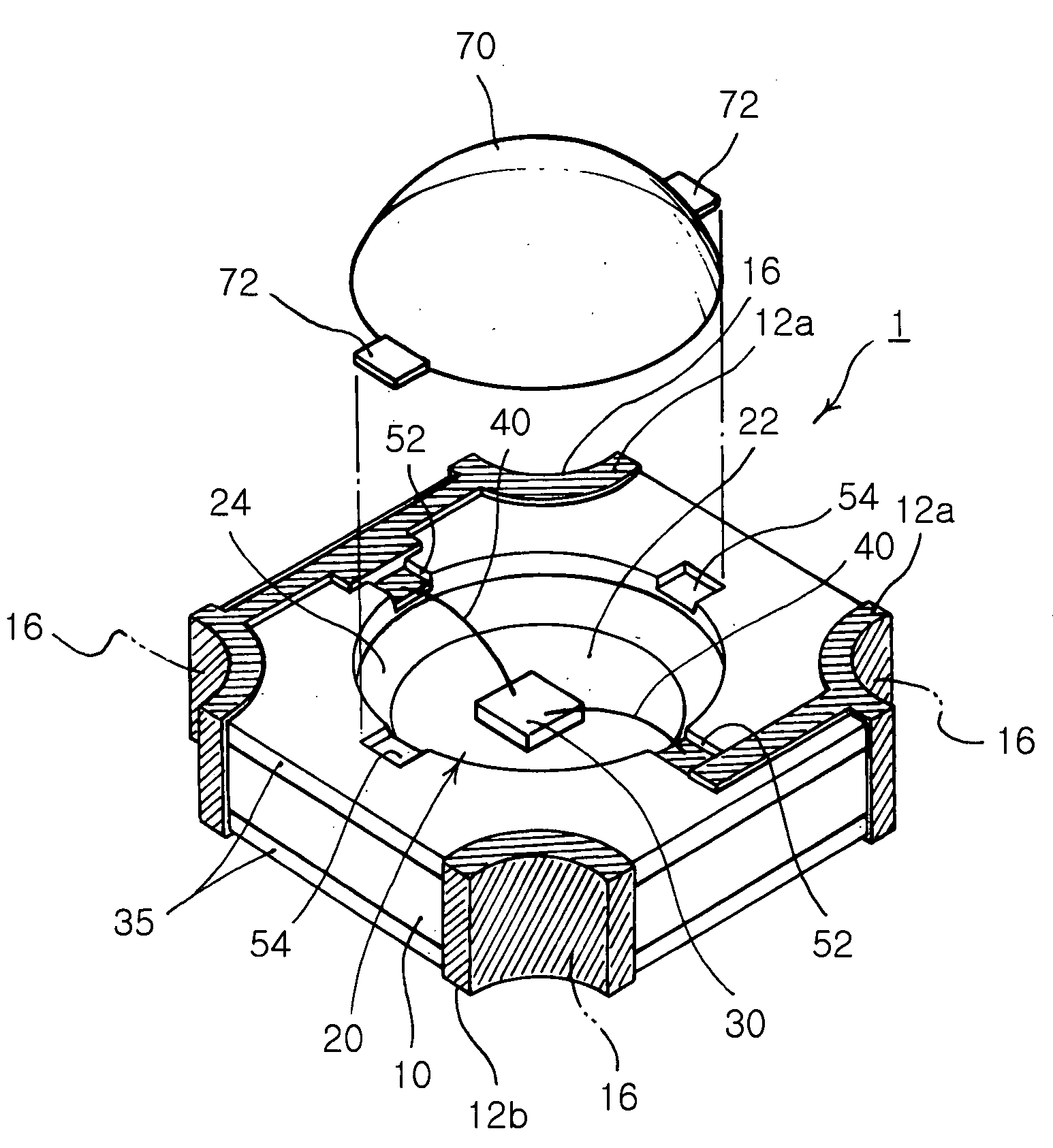
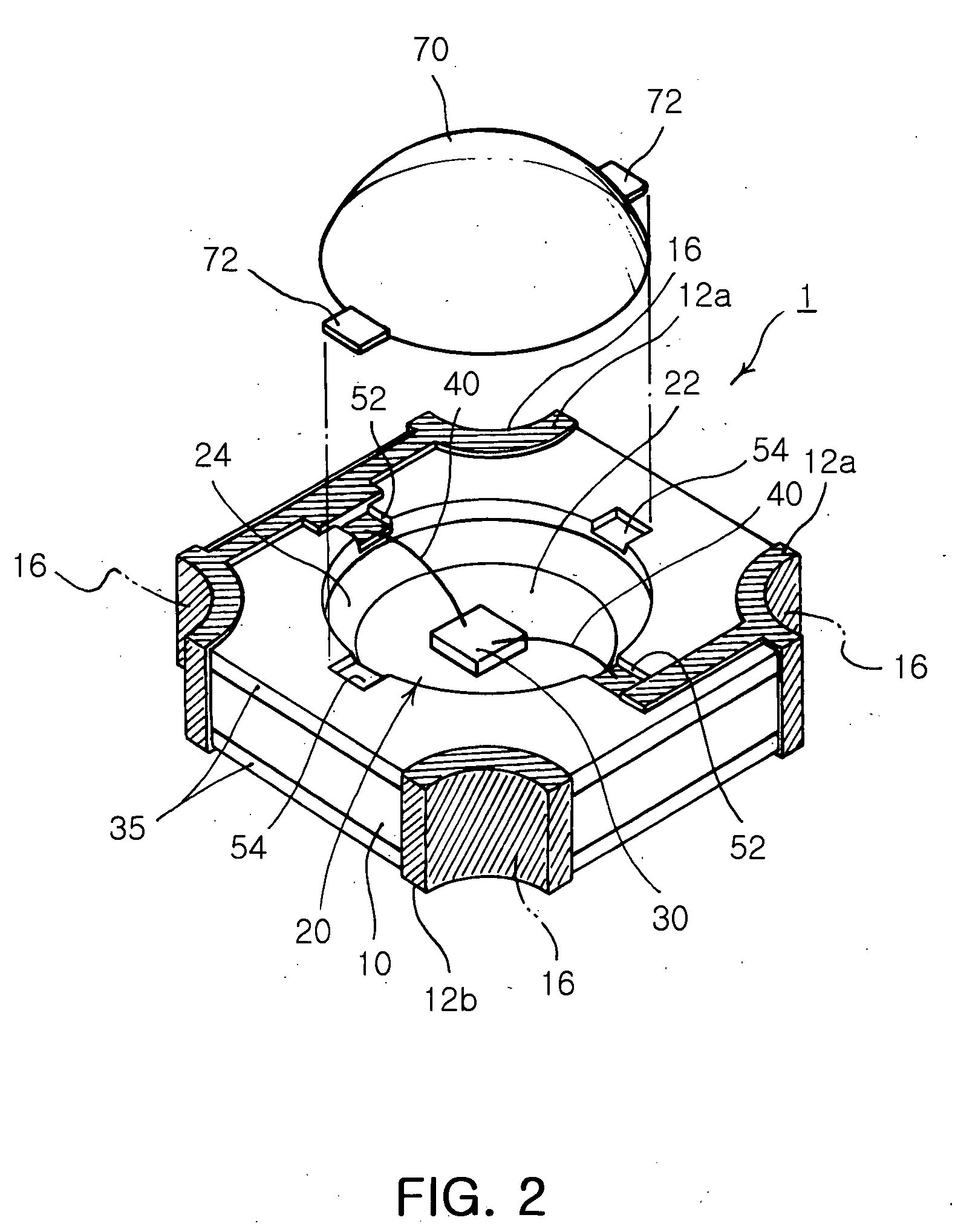
[0033]As shown in FIG. 2, an LED package 1 having an anodized insulation layer includes a substrate 10 made of an Al material. The substrate 10 is made of an Al material which is relatively low cost and easily manufactured.

[0034]The substrate 10 has a reflecting region 20 formed in a center thereof. The reflecting region 20 is a recessed groove formed by etching. As shown in FIG. 3, the reflecting region 20 is composed of a planar central reflecting area 22 where the light source 30 is mounted as described later, i.e., a die bonding reflecting area and an inclined reflecting area 24, i.e., a reflecting surface surrounding the central reflecting area 22.

[0035]In addition, electrode connecting grooves 52 connecting the electrodes of the LEDs of the light source 30 with wires 40 and lens assembly grooves 54 defining the location of the lens 70 described later...


PUM


Abstract

An LED package having an anodized insulation layer which increases heat radiation effect to prolong the lifetime LEDs and maintains high luminance and high output, and a method therefor. The LED package includes an Al substrate having a reflecting region and a light source mounted on the substrate and connected to patterned electrodes. The package also includes an anodized insulation layer formed between the patterned electrodes and the substrate and a lens covering over the light source of the substrate. The Al substrate provides superior heat radiation effect of the LED, thereby significantly increasing the lifetime and light emission efficiency of the LED.

Description

CLAIM OF PRIORITY[0001]This application claims the benefit of Korean Patent Application No. 2006-0031093 filed on Apr. 5, 2006, in the Korean Intellectual Property Office, the disclosure of which is incorporated herein by reference.BACKGROUND OF THE INVENTION[0002]1. Field of the Invention[0003]The present invention relates to a Light Emitting Diode (LED) package of high luminance and high output, which uses an LED as a light source and a method therefor. More particularly, the present invention relates to an LED package, which has a light source mounted in a reflecting region of an aluminum (Al) substrate that is anodized to have an insulation layer, thereby increasing the heat radiation effect of the LED during the light emission operation, prolonging the lifetime of the LED and maintaining high luminance and output of the LED, and to a fabrication method therefor.[0004]2. Description of the Related Art[0005]In general, as shown in FIG. 1, a conventional LED package having an LED ...

Claims


Application Information

Patent Timeline
Patent Type & Authority Applications(United States)
IPC IPC(8): H01L33/00H01L33/58H01L33/60H01L33/62H01L33/64
CPCH01L25/0753H01L33/483H01L33/58H01L33/62H01L33/641H01L2224/48091H01L2224/48227H01L2224/49171H01L2924/00014H01L2924/00
Inventor LEE, YOUNG KICHOI, SEOG MOONSHIN, SANG HYUN
Owner SAMSUNG ELECTRONICS CO LTD
Why Eureka
Try Eureka