Write margin improvement for SRAM cells with SiGe stressors

a technology of stressors and write margins, applied in the field of pmos devices with sige stressors, can solve the problems of pattern loading effects, adversely affecting the drive current of devices, severe degradation of carrier mobility, etc., and achieve the effect of reducing the drive current of pull-up pmos devices and improving the write margins of sram cells

Active Publication Date: 2007-10-11
TAIWAN SEMICON MFG CO LTD
View PDF2 Cites 42 Cited by
  • Summary
  • Abstract
  • Description
  • Claims
  • Application Information

AI Technical Summary

Benefits of technology

[0012] By reducing the drive currents of pull-up PMOS devices in SRAM cells, write margins of SRAM cells are improved. Meanwhile, PMOS devices in core circuit regions are not affected.

Problems solved by technology

Continued scaling of MOS devices results in severe degradation of carrier mobility, however, which in turn adversely affects the device drive current.
However, since the core circuit typically occupies a small region on a memory chip, SiGe stressors will only be formed in the small region, resulting in pattern loading effects and process difficulties for subsequent process steps.

Method used


Image

  • Write margin improvement for SRAM cells with SiGe stressors
  • Write margin improvement for SRAM cells with SiGe stressors
  • Write margin improvement for SRAM cells with SiGe stressors

Examples


Embodiment Construction

[0018] The making and using of the presently preferred embodiments are discussed in detail below. It should be appreciated, however, that the present invention provides many applicable inventive concepts that can be embodied in a wide variety of specific contexts. The specific embodiments discussed are merely illustrative of specific ways to make and use the invention, and do not limit the scope of the invention.

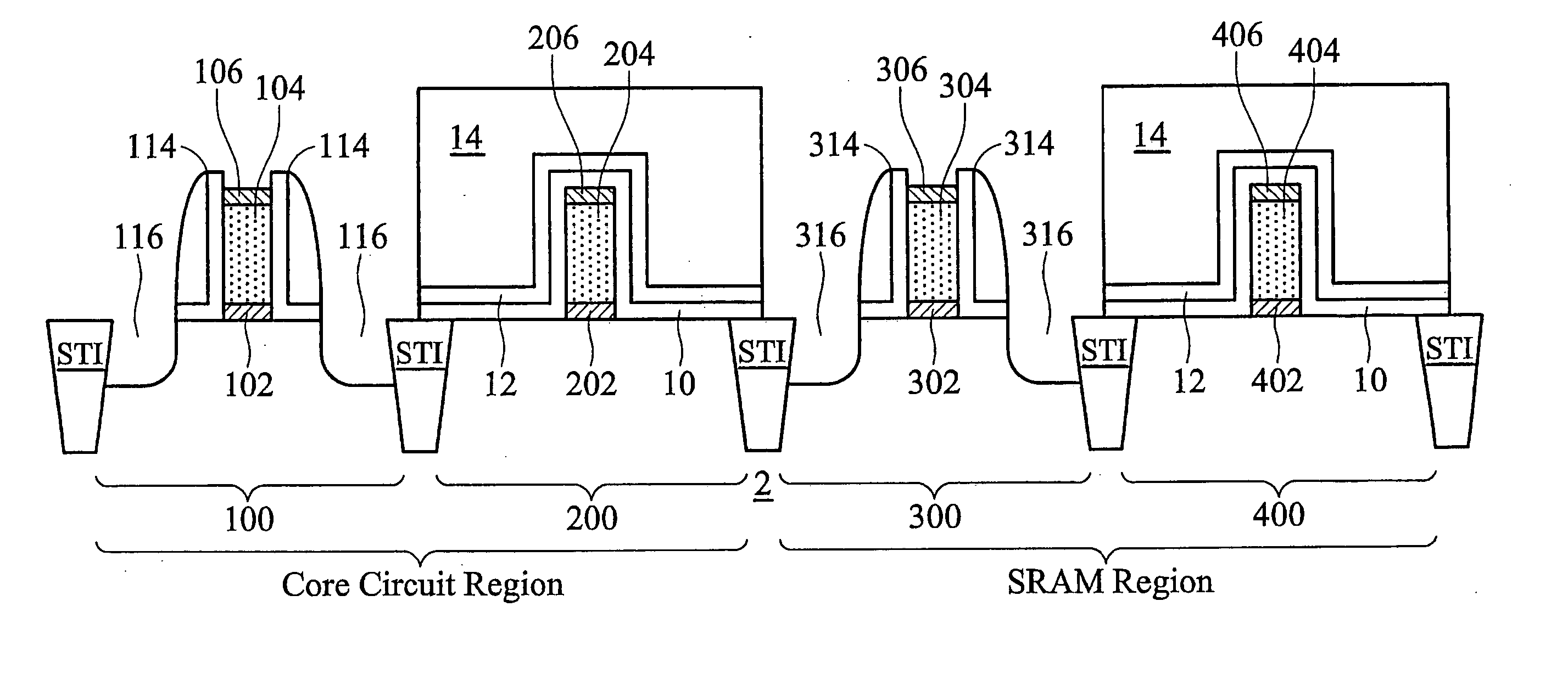
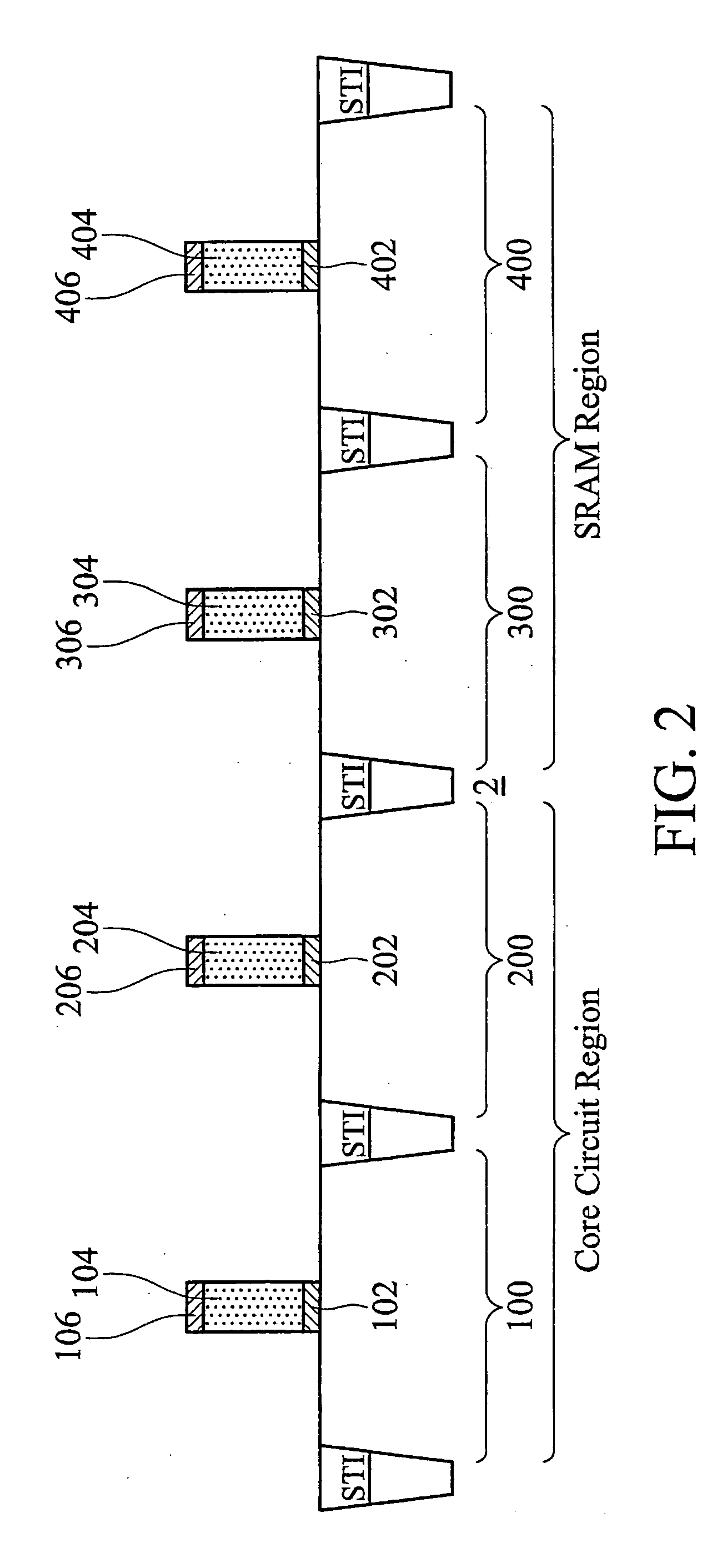
[0019] The intermediate stages of manufacturing a preferred embodiment of the present invention, which combines the formation of PMOS and NMOS devices for core circuits and SRAM cells, are illustrated. Throughout the various views and illustrative embodiments of the present invention, like reference numbers are used to designate like elements.

[0020]FIG. 2 illustrates a substrate 2, which includes a core circuit region and an SRAM region isolated by shallow trench isolation (STI) regions. Substrate 2 preferably comprises bulk silicon, although other commonly used materials ...


PUM


Abstract

A semiconductor structure including SRAM cells with improved write margins and a method for forming the same are provided. The semiconductor structure comprises a substrate including a core circuit and an SRAM cell. The SRAM cell includes a pull-up PMOS device that comprises a first source/drain region in the substrate, a first SiGe stressor having a portion overlapping at least a portion of the first source/drain region, and a first current-tuning region having a portion overlapping at least a portion of the first source/drain region. The core circuit comprises a core PMOS device that comprises a second source/drain region in the substrate, and a second SiGe stressor having a portion overlapping at least a portion of the second source/drain region. The core PMOS device is free of current-tuning regions.

Description

TECHNICAL FIELD [0001] This invention relates generally to semiconductor devices, and more particularly to PMOS devices with SiGe stressors, and even more particularly to methods of manufacturing pull-up PMOS devices in static random access memory cells. BACKGROUND [0002] Scaling of semiconductor devices (e.g., a metal-oxide semiconductor field-effect transistor) has enabled continued improvement in speed, performance, density, and cost per unit function of integrated circuits over the past few decades. In accordance with a design of the transistor and one of the inherent characteristics thereof, modulating a length of a channel region underlying a gate between a source and drain of the transistor alters a resistance associated with the channel region, thereby affecting a performance of the transistor. More specifically, shortening the length of the channel region reduces a source-to-drain resistance of the transistor, which, assuming other parameters are maintained relatively const...

Claims


Application Information

Patent Timeline
Patent Type & Authority Applications(United States)
IPC IPC(8): H01L29/94H01L29/76
CPCH01L27/1104H01L27/11H10B10/00H10B10/12
Inventor WANG, YIN-PINDIAZ, CARLOS H.
Owner TAIWAN SEMICON MFG CO LTD
Why Eureka
Try Eureka