Dynamic metrology sampling with wafer uniformity control

a technology of uniformity control and dynamic metrology, which is applied in the field of system and method of processing a wafer, can solve the problems of additional processing control problems and the structure of the semiconductor wafer not only reducing in siz

Inactive Publication Date: 2007-10-11
IBM CORP +1
View PDF14 Cites 25 Cited by
  • Summary
  • Abstract
  • Description
  • Claims
  • Application Information

AI Technical Summary

Benefits of technology

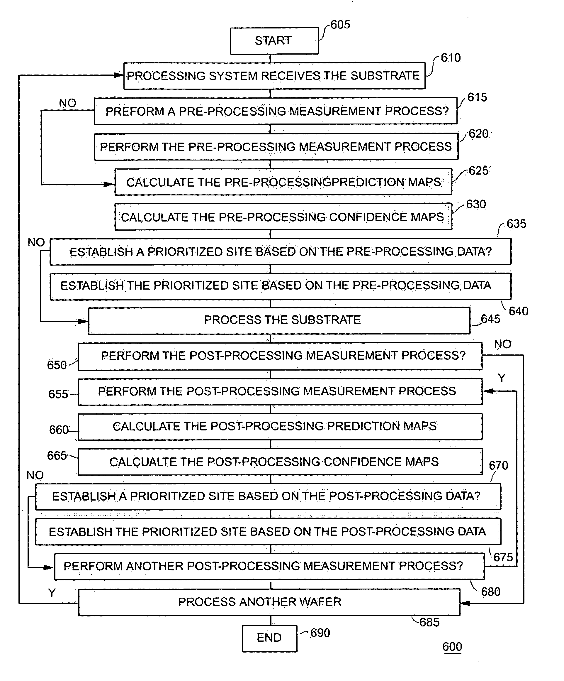
[0008] The principles of the present invention are directed to a method of processing a wafer, wherein the wafer includes a plurality of dies, each die having a patterned bi-layer mask thereon. The mask layer includes a soft mask layer and a hard mask layer. A pre-processing measurement map is created using measured metrology data for the wafer including metrology data for at least one isolated bi-layer structure on the wafer, metrology data for at least one nested bi-layer structure on the wafer, or mask data. A first pre-processing prediction map for the wafer is calculated based on the pre-processing measurement map. The f

Problems solved by technology

The structures on the semiconductor wafers have not only decreased in size but also have increased in density causing additional processing control problems.
Areas on semiconductor wafers have been iden

Method used


Image

  • Dynamic metrology sampling with wafer uniformity control
  • Dynamic metrology sampling with wafer uniformity control
  • Dynamic metrology sampling with wafer uniformity control

Examples


Embodiment Construction

[0028] In material processing methodologies, pattern etching comprises the application of a thin layer of light-sensitive material, such as photoresist, to a wafer that is subsequently patterned in order to provide a soft mask for transferring this pattern to the underlying material during etching. The patterning of the light-sensitive material generally involves exposure by a radiation source of the light-sensitive material using, for example, a microlithography system, followed by the removal of the irradiated regions of the light-sensitive material (as in the case of positive photoresist), or non-irradiated regions (as in the case of negative resist) using a developing solvent.

[0029] Additionally, single and / or multi-layer masks can be implemented. Soft mask and / or hard mask layers can be used. For example, when etching features using a soft mask top layer, the mask pattern in the soft mask layer is transferred to the hard mask layer using a separate etch step (hard mask open) p...


PUM


Abstract

A method of processing a wafer is presented that includes creating a pre-processing measurement map using measured metrology data for the wafer including metrology data for at least one isolated structure on the wafer, metrology data for at least one nested structure on the wafer, or mask data. At least one pre-processing prediction map is calculated for the wafer. A pre-processing confidence map is calculated for the wafer. The pre-processing confidence map includes a set of confidence data for the plurality of dies on the wafer. A prioritized measurement site is determined when the confidence data for one or more dies is not within the confidence limits. A new measurement recipe that includes the prioritized measurement site is then created.

Description

CROSS-REFERENCE TO RELATED APPLICATIONS [0001] This application is related to co-pending U.S. patent application Ser. No. 10 / 705,200, entitled “Processing System And Method For Chemically Treating A Wafer”, filed on Nov. 12, 2003; co-pending U.S. patent application Ser. No. 10 / 704,969, entitled “Processing System And Method For Thermally Treating A Wafer”, filed on Nov. 12, 2003; co-pending U.S. patent application Ser. No. 10 / 705,397, entitled “Method And Apparatus for Thermally Insulating Adjacent Temperature Controlled Chambers”, filed on Nov. 12, 2003; co-pending U.S. patent application Ser. No. 10 / 944,463, entitled “Iso / Nested Cascading Trim Control With Model Feedback Updates”; filed Sep. 20, 2004; co-pending U.S. patent application Ser. No. 11 / 046,903, entitled “Iso / Nested Control For Soft Mask Processing”; filed Feb. 1, 2005; U.S. patent application Ser. No. ______, Attorney Docket No. 313530-P0024, entitled “Dynamic Metrology Sampling With Wafer Uniformity Control”, filed on...

Claims


Application Information

Patent Timeline
IPC IPC(8): G06K9/00
CPCG03F7/70625G03F7/70525
Inventor FUNK, MERRITTSUNDARARAJAN, RADHAPRAGER, DANIEL JOSEPHNATZLE, WESLEY
Owner IBM CORP
Why Eureka
Try Eureka