Method for fabricating active matrix organic light emitting diode display device and structure of such device

a technology of organic light-emitting diodes and display devices, which is applied in the direction of diodes, semiconductor devices, electrical devices, etc., can solve the problems of complex fabrication of conventional amoled display devices b>200/b> having coa structure and the unlikely reduction of production costs of such devices, so as to simplify the manufacturing procedure and reduce production costs

Inactive Publication Date: 2007-10-11
CHUNGHWA PICTURE TUBES LTD
View PDF4 Cites 22 Cited by
  • Summary
  • Abstract
  • Description
  • Claims
  • Application Information

AI Technical Summary

Benefits of technology

[0029] The present invention employs a half-tone mask to pattern the first, the second and the third color photoresistant layers, thus the subsequently obtained first, second and third color filter layers can be used as pixel defining layers and etching masks for making the contact window openings. The method for fabricating an AMOLED display device is adapted for simplifying fabricating procedures and lowering production cost by skipping over the process of making pixel defining layers and etching masks for making the contact window openings.

Problems solved by technology

According to the foregoing, the fabrication of the conventional AMOLED display device 200 having COA structure is complicated and the production cost thereof is unlikely to be lowered.

Method used


Image

  • Method for fabricating active matrix organic light emitting diode display device and structure of such device
  • Method for fabricating active matrix organic light emitting diode display device and structure of such device
  • Method for fabricating active matrix organic light emitting diode display device and structure of such device

Examples


Embodiment Construction

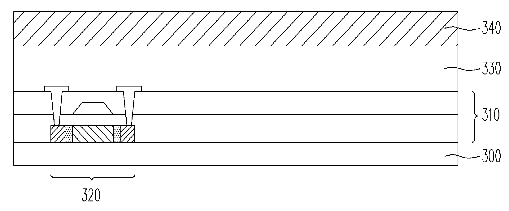
[0034]FIGS. 2A through 2H are schematic cross-sectional views illustrating a process for fabricating an AMOLED display device according to an embodiment of the present invention. Referring to FIGS. 2A through 2H, the method for fabricating an AMOLED display device according to an embodiment of the present invention is illustrated as below.

[0035] First, a substrate 300 is provided as shown in FIG. 2A. The substrate 300, for example, is glass substrate, quartz substrate or flexible substrate. Then, referring to FIG. 2A again, a device layer 310 is configured on the substrate. The device layer 310 includes a plurality of active devices 320 (only one shown in FIG. 2A). According to an embodiment of the invention, the active devices 320, for example, are thin film transistors (TFTs). And, the device layer 310 includes a plurality of scan lines (not shown) and data lines (not shown), by which the active devices 320 can be driven. The method for forming the device layer 310 is utilized by...


PUM


Abstract

A method for fabricating an AMOLED display device is provided. A substrate is provided. A device layer having multiple active devices is formed on the substrate. A flat layer is configured on the device layer. A first, a second and a third color photoresistant layers are respectively configured on the flat layer and are patterned to form a first, a second and a third color filter layers. The first, the second and the third color filter layers respectively define a first, a second and a third pixel areas and are used for etching masks to etch the flat layer for exposing parts of the active devices. A first, a second and a third pixel electrode are respectively configured in the mentioned pixel areas and are electrically connected with the active devices. A first, a second and a third organic light emitting layers are respectively configured on the mentioned pixel electrodes.

Description

BACKGROUND OF THE INVENTION [0001] 1. Field of the Invention [0002] The present invention relates to a method for fabricating an Active Matrix Organic Light Emitting Diode (AMOLED) display device and a structure of such device, and particularly to a method for fabricating an AMOLED display device and a structure thereof, in which color filter layers are processed by a half-tone mask. [0003] 2. Description of Related Art [0004] An Organic Light Emitting Diode (OLED) is a semiconductor device capable of efficiently converting electrical energy into optical energy. OLEDs are wildly used as luminous elements in indication lights, display panels and optical reading / writing heads. Wherein, OLED display devices, having advantages such as free-viewing angles, simple processing, low production cost, fast response, wide operation temperature range and full color displaying, meet the demands of modern display devices in the multimedia field. So, in recent years, OLEDs are being enthusiasticall...

Claims


Application Information

Patent Timeline
Patent Type & Authority Applications(United States)
IPC IPC(8): H01L51/40
CPCH01L27/1214H01L51/56H01L27/3244H01L27/322H01L27/1288H10K59/38H10K59/12H10K71/00
Inventor TENG, TE-HUACHEN, CHIA-CHIENLU, FANG-YIWU, BING-WEIYANG, YUN-PEI
Owner CHUNGHWA PICTURE TUBES LTD
Why Eureka
Try Eureka