Field effect transistor with independently biased gates

a field effect transistor and gate technology, applied in the field of field effect transistors, can solve the problems of device substantially constant transconductance, and high breakdown, and achieve the effects of constant transconductance, high breakdown, and high degree of linearity

Inactive Publication Date: 2007-10-18
MASSACHUSETTS UNIV OF
View PDF2 Cites 55 Cited by
  • Summary
  • Abstract
  • Description
  • Claims
  • Application Information

AI Technical Summary

Benefits of technology

[0004] Embodiments of the invention relate to tailoring the electric field in the channel region of a FET by appropriately positioning and biasing at least two gates of the FET. In accordance with the invention, each of the gates may be biased independently. For example, the same AC voltage may be applied to each gate, but each gate may biased at a different DC voltage. In one aspect of the invention, the electric field may be tailored by positioning one of the gates closer to the channel than the other gate. Using a FET with independently biased gates may enable providing a uniform electric field in the channel region of the FET. Furthermore, such a device may exhibit substantially constant transconductance, a high degree of linearity, and high breakdown, i.e., Early voltage. Constant transconductance provides a high degree of linearity, which can be particularly beneficial for amplifier applications in which linearity across a broad range of gate voltages is desirable.

Problems solved by technology

Furthermore, such a device may exhibit substantially constant transconductance, a high degree of linearity, and high breakdown, i.e., Early voltage.

Method used


Image

  • Field effect transistor with independently biased gates
  • Field effect transistor with independently biased gates
  • Field effect transistor with independently biased gates

Examples


Embodiment Construction

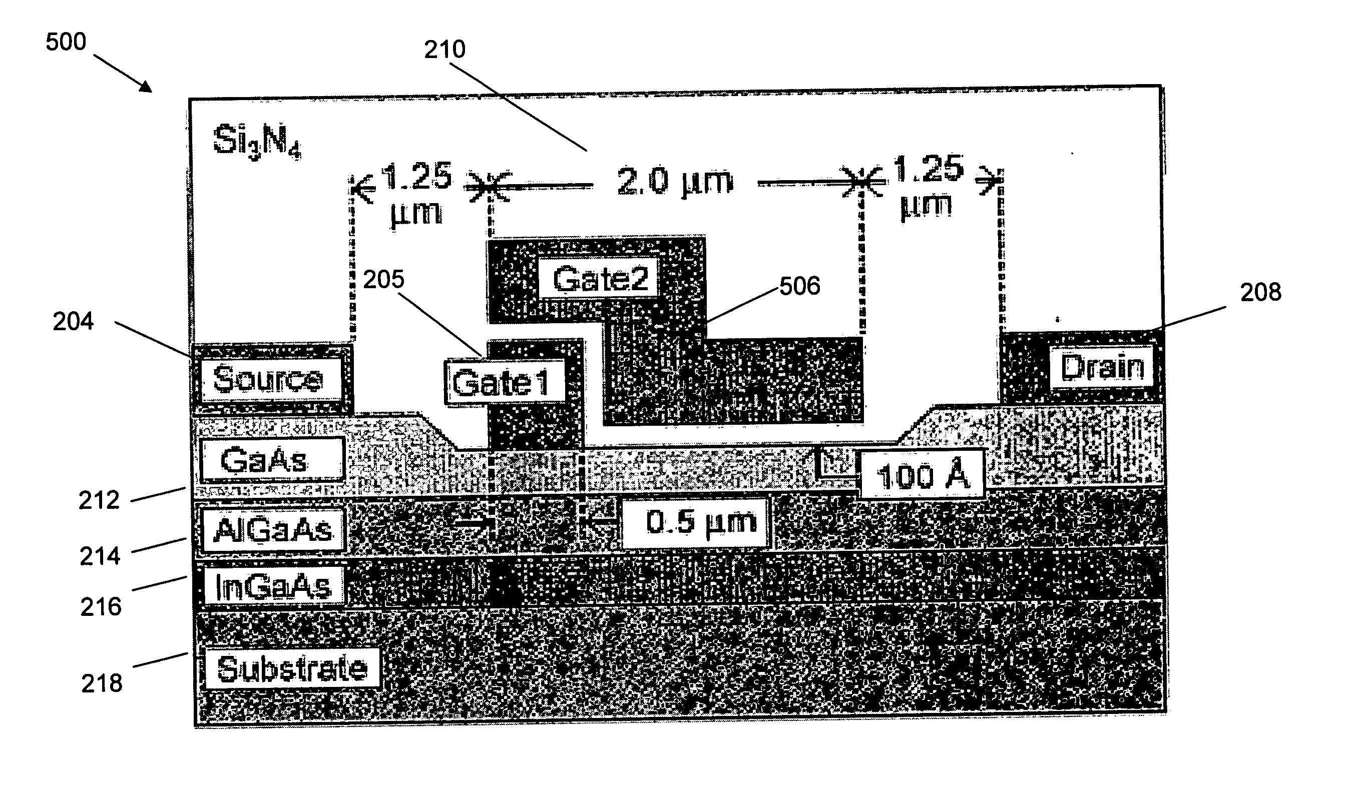
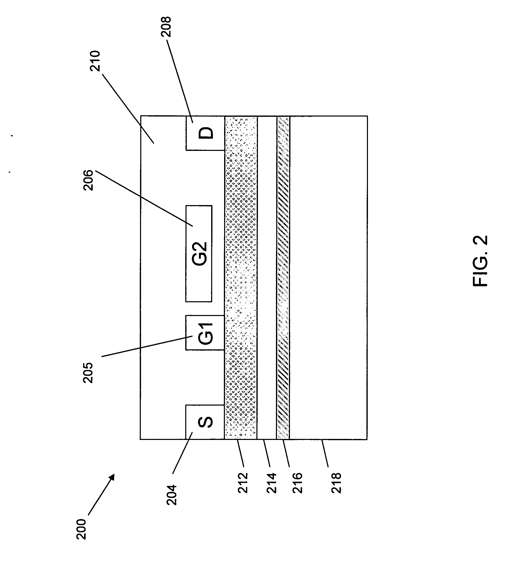
[0016] In accordance with some embodiments of the invention, a FET having at least two independently biased gates enables tailoring the electric field in the channel region of the FET. One of the gates may be positioned closer to the channel than the other gate. Using such a configuration, the electric field may be tailored so that it is substantially uniform in the channel region, which can improve the performance of the FET. For example, the FET can achieve substantially constant transconductance. Embodiments of the invention may be useful in a variety of amplifiers, mixers, switches or any other suitable circuits.

[0017]FIG. 2 is a cross-section of a pseudomorphic high-electron-mobility transistor (pHEMT) according to one embodiment of the invention. In this embodiment, pHEMT 200 includes a source 204, drain 208, a first gate 205 and a second gate 206. Source 204, drain 208, first gate 205 and second gate 206 may be metallizations formed of any suitable material, e.g., a metal su...


PUM


Abstract

A field effect transistor (FET) having at least two independently biased gates can provide uniform electric field in the channel region of the FET. The same AC voltage may be applied to each gate for modulating the FET. One of the gates is positioned closer to the channel region than the other gate. Such a FET allows tailoring the electric field in the channel region of the FET so that it is substantially uniform. The FET exhibits desirable performance characteristics, including having a constant transconductance.

Description

BACKGROUND OF INVENTION [0001] Field effect transistors (FETs) are semiconductor devices used in a wide variety of electronics applications. A FET has three terminals: a source, a drain and a gate. During operation of the FET, current flows between source and drain terminals through a channel region. The gate electrode, positioned between the source and the drain, enables the current through the FET to be controlled based on the strength of the signal applied to the gate. The signal and bias present at the gate, source and drain determines the electric field profile in the channel region between the source and the drain. The performance of the FET, e.g., factors such as current gain, carrier mobility, and transconductance (gm), are determined by the profile of the electric field in the channel region. [0002] In conventional FETs, the strength of the electric field varies over the length of the channel, being typically weaker near the source and stronger near the drain (in depletion ...

Claims


Application Information

Patent Timeline
Patent Type & Authority Applications(United States)
IPC IPC(8): H01L31/00
CPCH01L29/7783H01L29/42316
Inventor MIL'SHTEIN, SAMSONPALMA, JOHN F.
Owner MASSACHUSETTS UNIV OF
Why Eureka
Try Eureka