

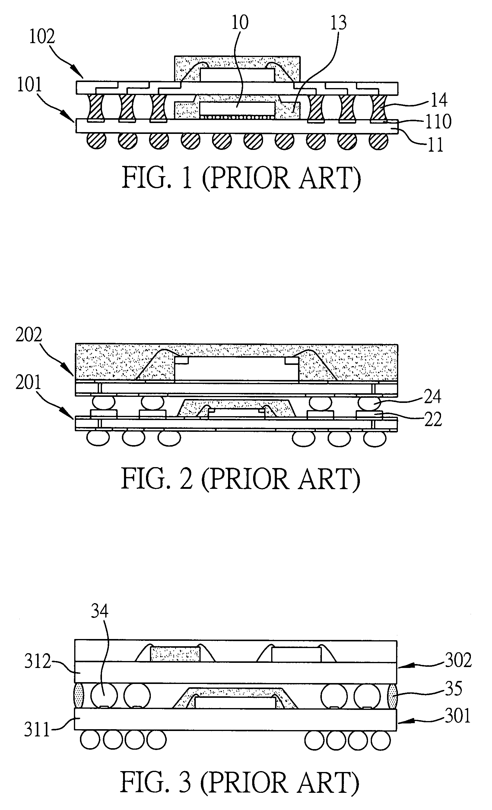
Stack structure of semiconductor packages and method for fabricating the stack structure
a stack structure and semiconductor technology, applied in the direction of semiconductor devices, semiconductor/solid-state device details, electrical apparatus, etc., can solve the problems of failure of electrical connection between the first and second semiconductor packages, increase the complexity of the fabrication increase the fabrication cost and complexity of the fabrication process for the stack structure, and avoid the increase in the complexity of the fabrication process
- Summary
- Abstract
- Description
- Claims
- Application Information
AI Technical Summary
Benefits of technology
Problems solved by technology
Method used
Image

Examples
first embodiment
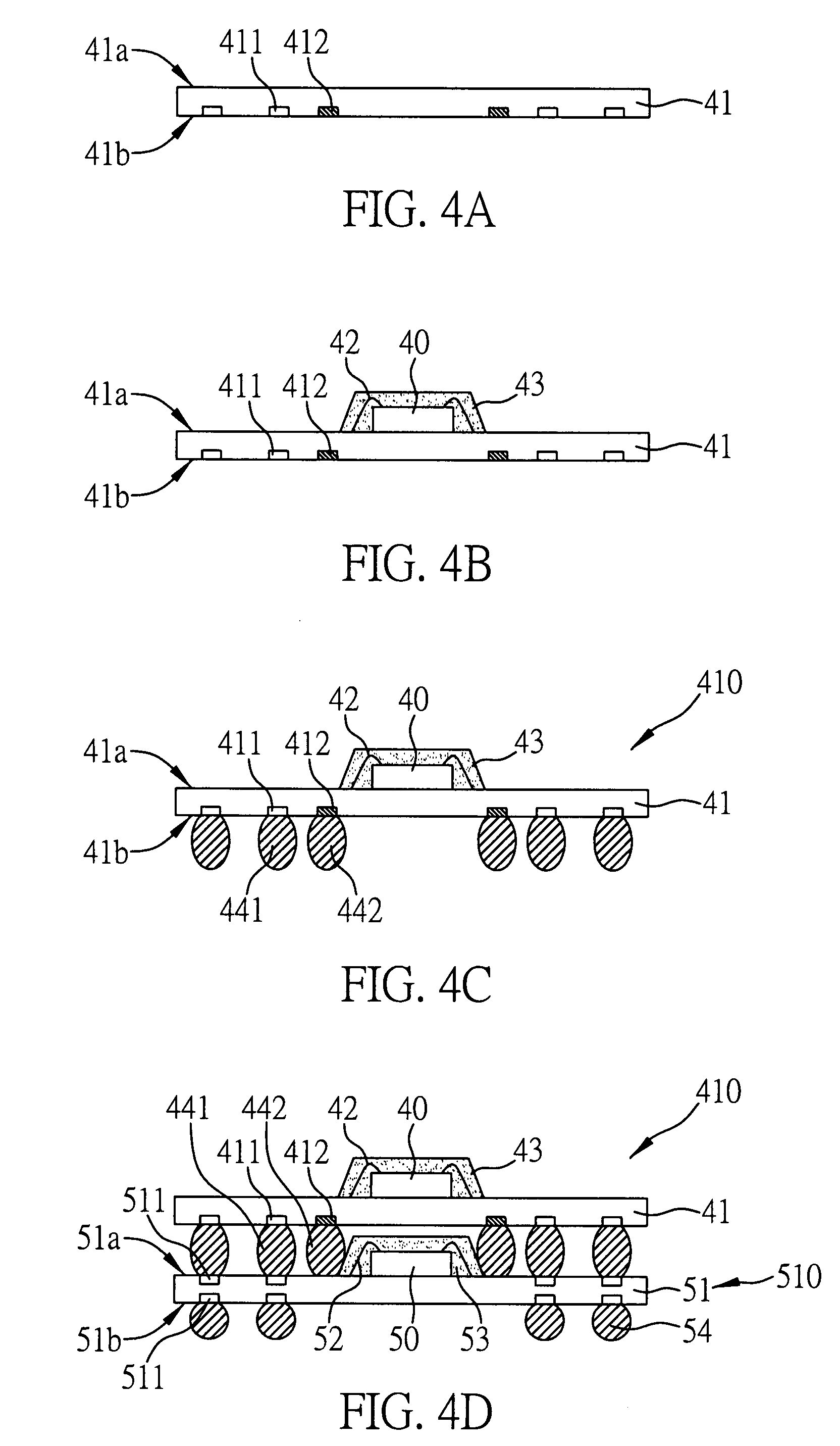
[0026]FIGS. 4A to 4D are cross-sectional views of a stack structure of semiconductor packages and a method for fabricating the stack structure in accordance with a first embodiment of the present invention.
[0027]As shown in FIG. 4A, a substrate 41 having a first surface 41a and a second surface 41b opposite to the first surface 41a is provided, wherein a plurality of electrical connection pads 411 and dummy pads 412 are formed on the second surface 41b of the substrate 41. The substrate 41 is a substrate of an upper semiconductor package that is to be subsequently stacked on a fabricated lower semiconductor package. The substrate 41 is, for example, a ball grid array (BGA) substrate.
[0028]Also referring to FIG. 5A showing the second surface 41b of the substrate 41 of FIG. 4A, the plurality of electrical connection pads 411 serve as electrical input / output (I / O) pads and are peripherally located in a peripheral portion of the second surface 41b of the substrate 41, and the plurality ...
second embodiment
[0037]FIGS. 6A and 6B show a second surface of a substrate of an upper semiconductor package in accordance with a second embodiment of the present invention.
[0038]A stack structure of semiconductor packages and a method for fabricating the stack structure in the second embodiment are similar to those in the aforementioned first embodiment, with a primary difference in that, as shown in FIGS. 6A and 6B for the second embodiment, the dummy pads 412 formed on the second surface 41b of the substrate of the upper semiconductor package are located at positions corresponding to those closely adjacent to corners of the encapsulant (its projection to the second surface 41b is shown by the dashed lines) of the lower semiconductor package and further extended along the edges forming the corners of the encapsulant, thereby forming a continuous arrangement of the dummy pads 412 around each corner of the region encompassed by the dashed lines shown in FIG. 6A. As such, the solder balls, which are...
third embodiment
[0039]FIG. 7 is a cross-sectional view of a stack structure of semiconductor packages in accordance with a third embodiment of the present invention.
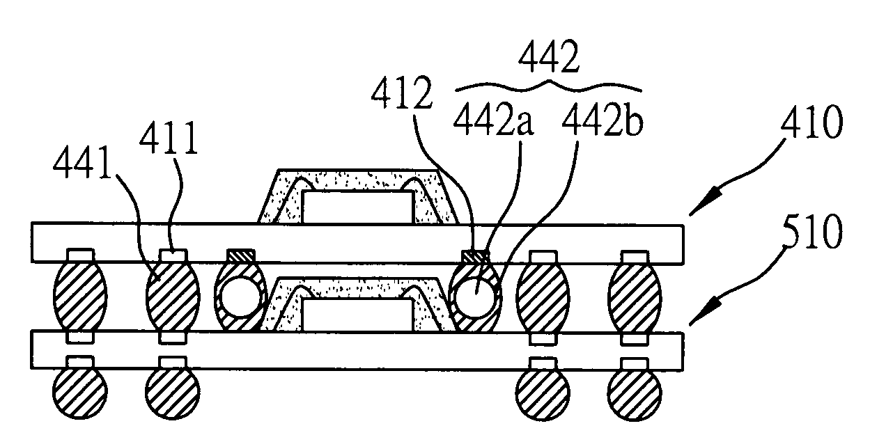
[0040]The stack structure of semiconductor packages of the third embodiment is similar to those of the aforementioned embodiments, with a primary difference in that, as shown in FIG. 7 for the third embodiment, the solder balls 442 implanted to the dummy pads 412 of the second surface 41b of the substrate of the upper semiconductor package 410 are smaller in size than the solder ball 441 implanted to the electrical connection pads 411, as long as the solder balls 422 implanted to the dummy pads 412 can surround and confine the encapsulant 53 of the lower semiconductor package 510, so as to prevent misalignment between the upper and lower semiconductor packages 410, 510.
PUM
 Abstract
Description
Claims
Application Information