Printed fourier filtering in optical inspection tools

a fourier filter and optical inspection technology, applied in the field of printed fourier filtering in optical inspection tools, can solve the problems of inability to meet the requirements of the application,

Active Publication Date: 2007-10-25
APPLIED MATERIALS SOUTH EAST ASIA PTE +1
View PDF99 Cites 15 Cited by
  • Summary
  • Abstract
  • Description
  • Claims
  • Application Information

AI Technical Summary

Benefits of technology

[0009] The filter masks may be printed using a printer including a loading stage which may hold at least one filter substrate, or a plurality of such substrates. The substrates may be moved using a conveyor to a printing stage including at least one inkjet printing head. The printer components may be housed in a substan

Problems solved by technology

The comparison of like fields of view can thus reveal irregularities which could indicate a defect.
However, prior Fourier filtering methodologies may be less than ideal when utilized in the field.
A reconfigurable filter is one way to meet the high demand for filters in such an environment, but such filters can introduce an additional level of complexity (and thus point of failure) into an already-complex environment.
Reconfigurable Fourier filters based on MEMS and LCD technologies have been proposed for use in optical inspection tools, but such filters may not always be practical for certain applications.
For instan

Method used


Image

  • Printed fourier filtering in optical inspection tools
  • Printed fourier filtering in optical inspection tools
  • Printed fourier filtering in optical inspection tools

Examples


Embodiment Construction

[0022] Reference will now be made in detail to present embodiments of the present invention, one or more examples of which are illustrated in the accompanying drawings, with like numerals representing substantially identical structural elements. Each example is provided by way of explanation, and not as a limitation. In fact, it will be apparent to those skilled in the art that modifications and variations can be made without departing from the scope or spirit of the disclosure and claims. For instance, features illustrated or described as part of one embodiment may be used on another embodiment to yield a still further embodiment. Thus, it is intended that the invention disclosed herein includes modifications and variations as come within the scope of the appended claims and their equivalents.

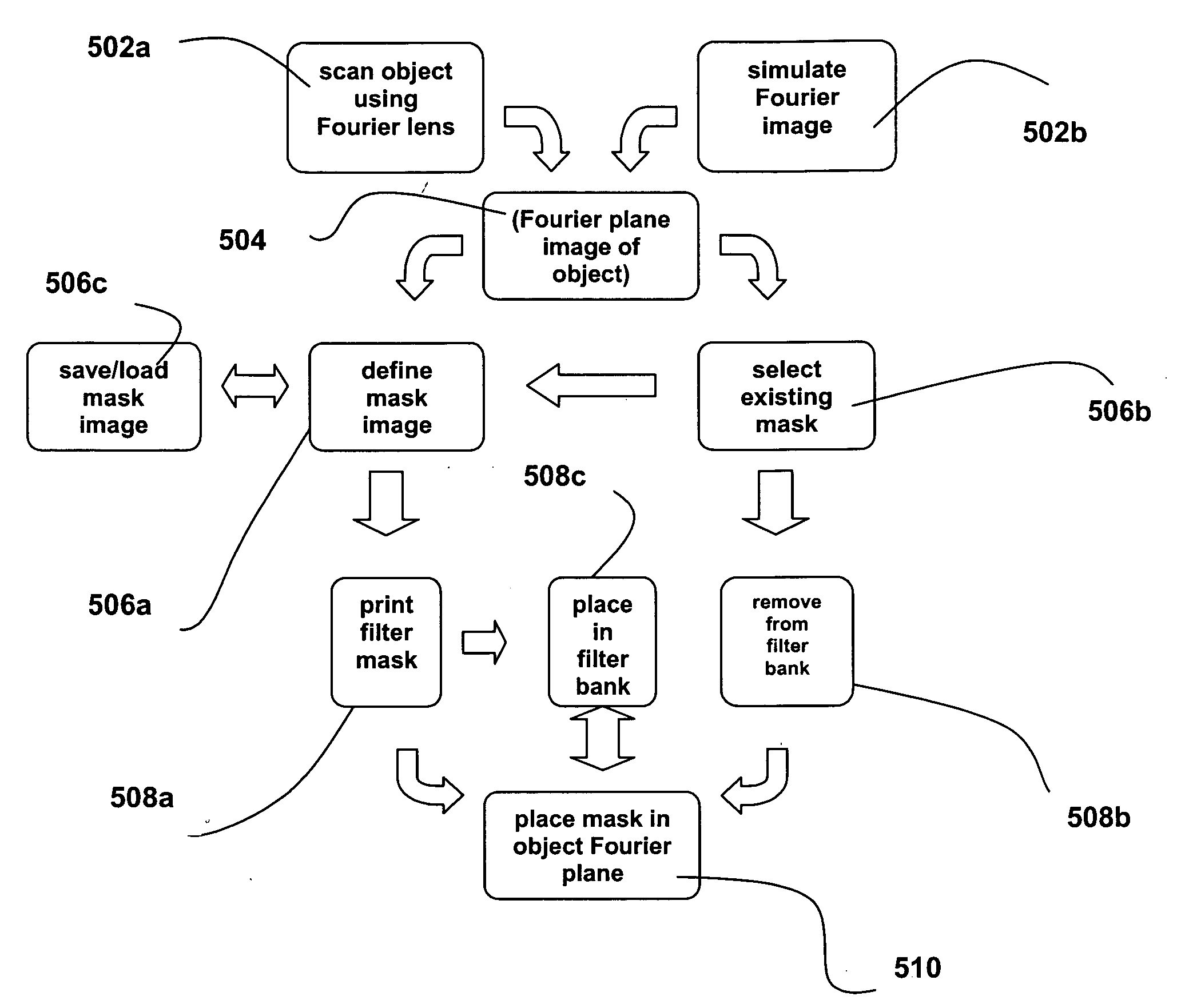
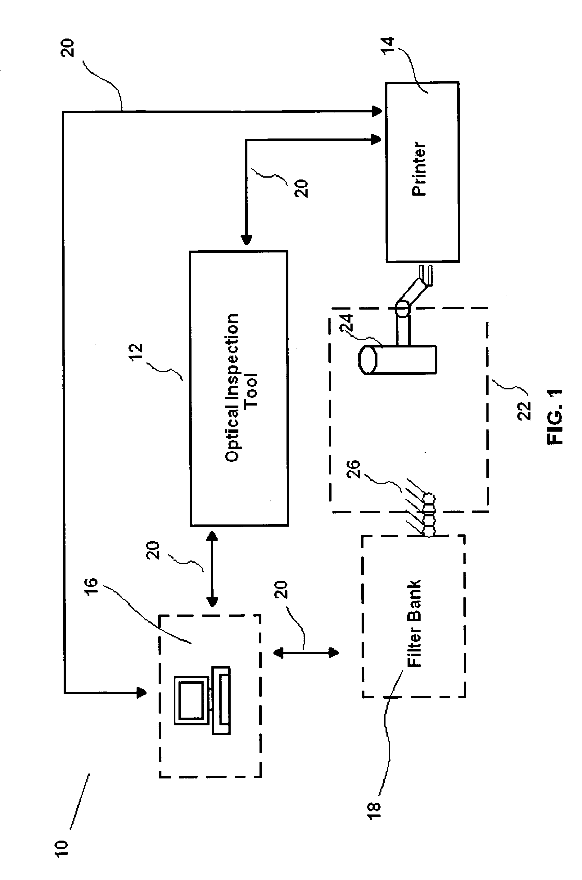
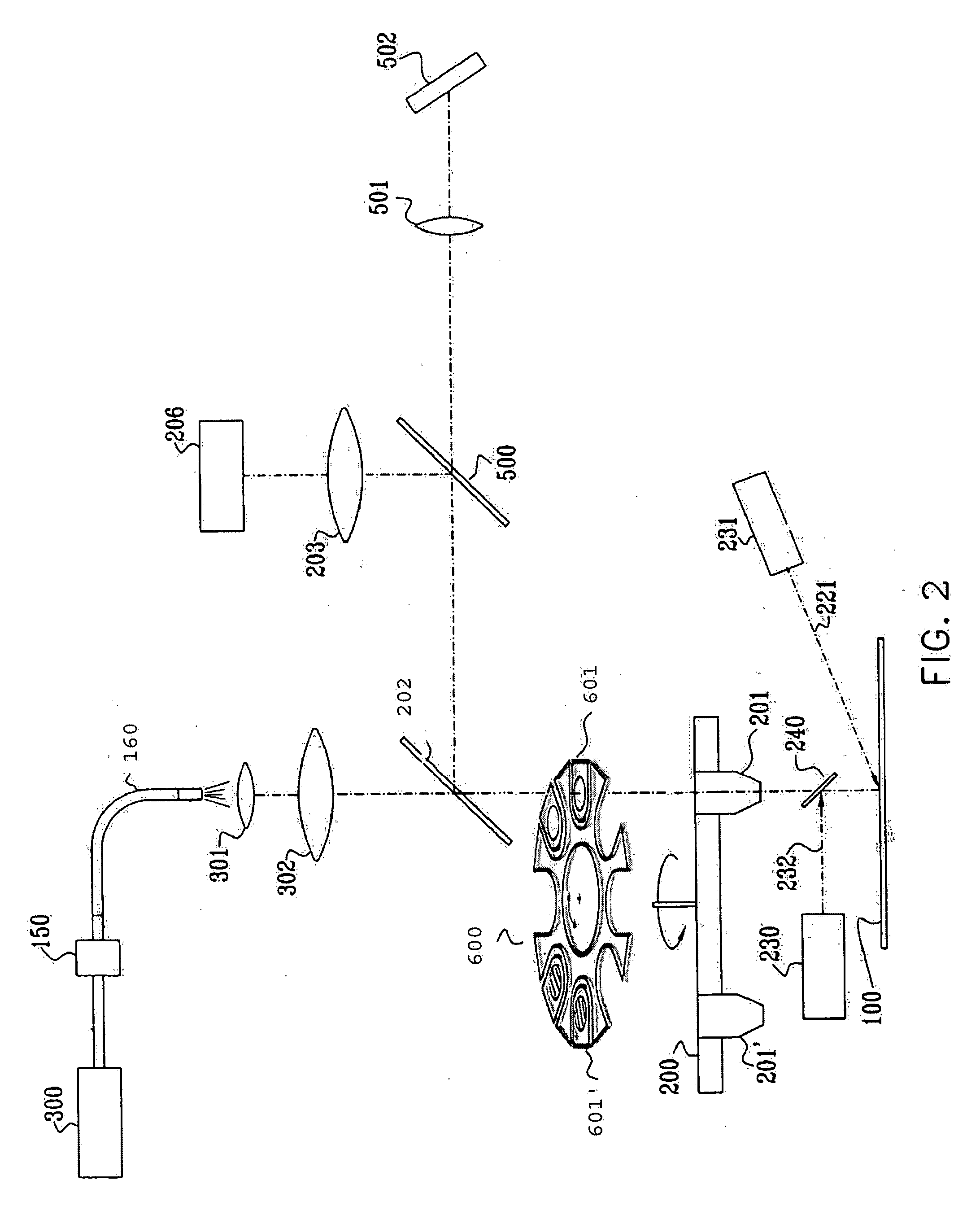
[0023]FIG. 1 illustrates an exemplary optical inspection system 10 including a spatial filter mask printer 14 operably connected to, or integrated as part of, an optical inspection tool 12. T...


PUM


Abstract

A spatial mask printer may be used in conjunction with an optical inspection tool. The tool can be used to obtain a Fourier image of an inspected object, and a filter mask image can be designed to block certain aspects of the object's image in the Fourier plane corresponding to repetitive aspects of the imaged object. The filter mask image can then be printed and used in the tool during the inspection process. The mask image may be designed by hand or by computer and may be stored for later use. Filters may be automatically placed into the optical path of the inspection tool by a filter wheel, or may be housed in other filter banks. The printer may be configured to operate in a clean room environment, and may be integrated into the optical inspection tool.

Description

BACKGROUND OF THE INVENTION [0001] In the semiconductor industry, devices are fabricated by a number of processes to produce precisely-defined structures of an ever-decreasing size. Even the slightest structural defect can ruin a semiconductor device, and so to avoid losses of time and effort, detection of defects is critical before a defective device is mass-produced or further processes are performed on a defective wafer. Fast, on-line detection of wafer defects is possible through the use of optical wafer inspection systems. For example, in one type of system, a two-dimensional image of a selected field of view of a wafer is obtained, and that field of view is compared to another view which, under ideal conditions, should be identical. The comparison of like fields of view can thus reveal irregularities which could indicate a defect. [0002] Generally speaking, a semiconductor wafer may include a number of repetitive patterns, and any defects in the semiconductor wafer will genera...

Claims


Application Information

Patent Timeline
IPC IPC(8): G06K9/76G06K15/00
CPCG01N21/95623G06K2209/19G06K9/741G06V10/89G06V2201/06
Inventor FUCHS, DAN T.SILBERSTEIN, SHAI
Owner APPLIED MATERIALS SOUTH EAST ASIA PTE
Why Eureka
Try Eureka