Semiconductor memory apparatus capable of reducing ground noise
a memory apparatus and semiconductor technology, applied in the field of semiconductor memory apparatus, can solve the problems of increasing the leak current of the respective control blocks in the bank, and increasing the amount of ground noise due to the activation operation of the selected bank. , to achieve the effect of reducing an influence and stable operation
- Summary
- Abstract
- Description
- Claims
- Application Information
AI Technical Summary
Benefits of technology
Problems solved by technology
Method used
Image
Examples
second embodiment
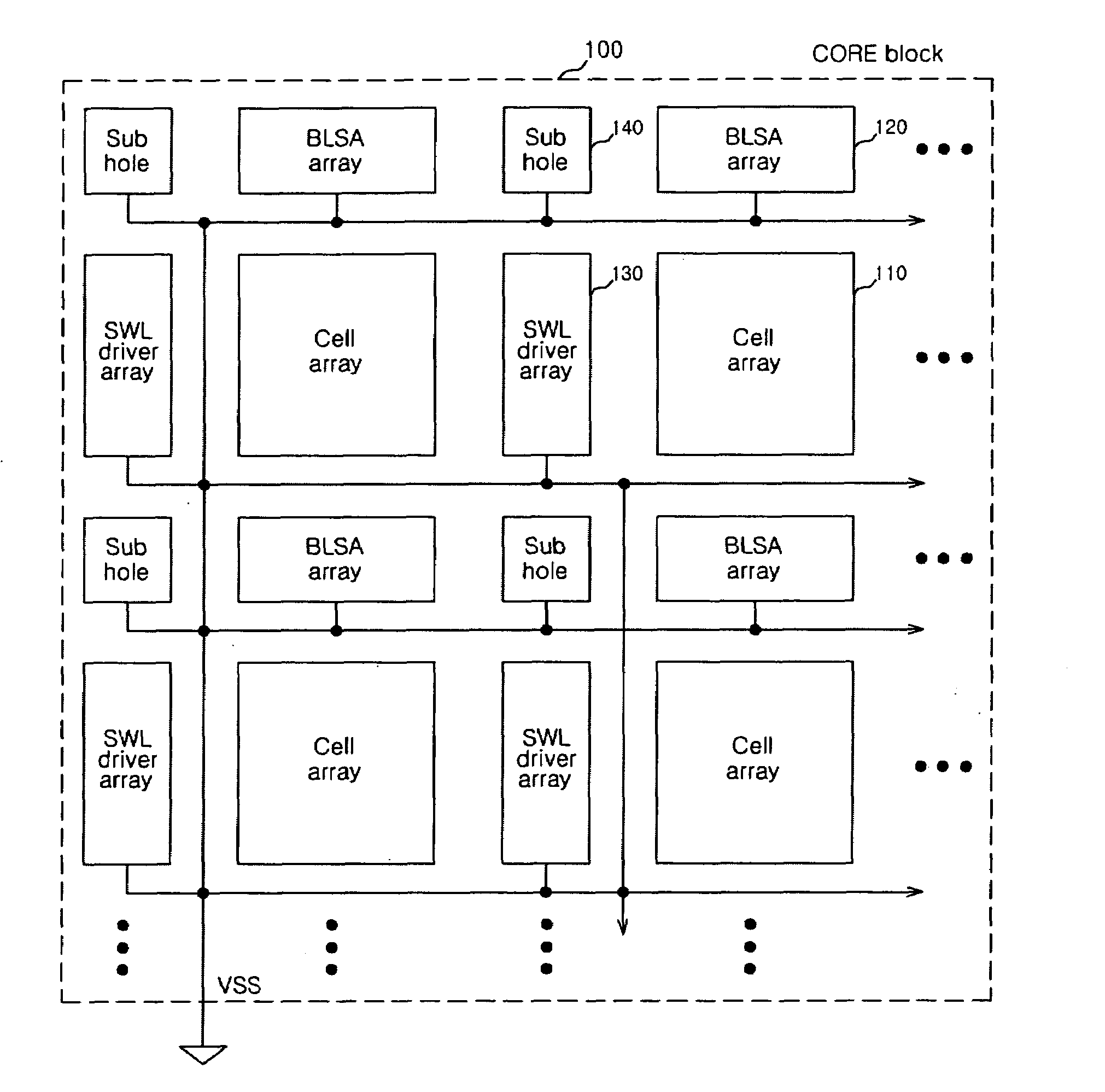
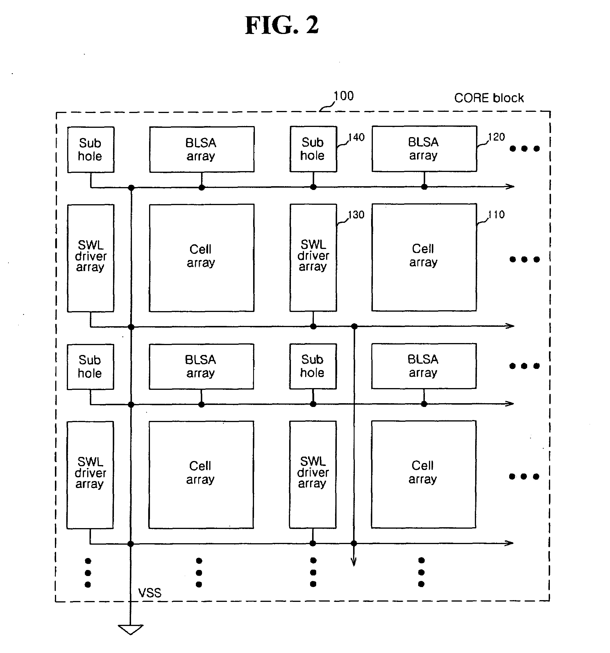
[0071]According to the structure of the second embodiment shown in FIG. 6, the ground line VSSW connected to the sub word line driver array in the core block 100 is directly connected to the ground line VSS (that is, node A) at the outside of the bank BANK, and the ground line VSSA is controlled through the switch SW-2. The reason why the ground line VSSW is not controlled by the block control unit 500 is because the sub word line SWL maintains a level of a ground power supply when it is not activated, and thus data of a cell can be easily maintained.
third embodiment
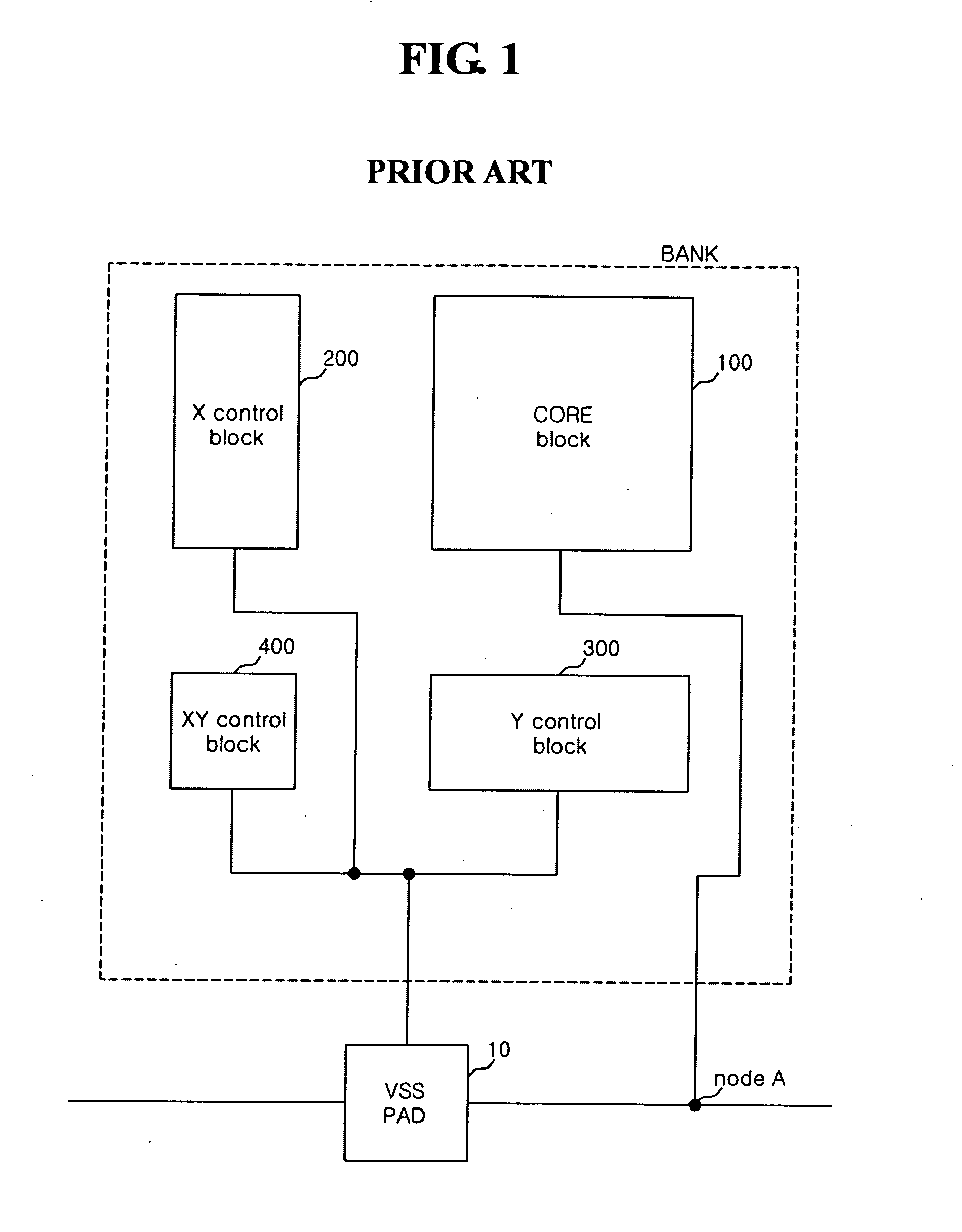
[0072]FIG. 7 is a block diagram illustrating a third embodiment of the invention. A semiconductor memory apparatus according to the invention shown in FIG. 7 includes a bank BANK that has a core block where a memory cell array is disposed and a control block to drive the memory cell array; a ground power supply pad 10 that is supplied with a ground power supply VSS through a ground line; a switch SW-3 that connects between the ground power supply pad 10 and the control block; and a block control unit 500 that controls an on / off operation of the switch SW-3.
[0073]The control block includes a row control block 200 that drives a row address path of the core block 100, a column control block 300 that drives a column address path of the core block 100, and a bank internal control block 400 that controls the row control block 200 and the column control block 300 according to a bank selection command. The row control block 200, the column control block 300, and the bank internal control bl...
fourth embodiment
[0078]According to the structure of the fourth embodiment shown in FIG. 8, the switch SW-4 that is controlled by an output signal bnoff of the bank control unit 600, is provided between the ground power supply pad 10 and the whole bank (whole block 100 to 400), such that an amount of leak current consumed by each of the core block 100, the row control block 200, the column control block 300, and the bank internal control block 400 forming the bank BANK is reduced. Further, all of blocks in the bank are not affected by ground noise transmitted from the outside of the bank BANK.
[0079]The embodiments shown in FIGS. 3, 6, and 7 illustrate a scheme that controls blocks, and the embodiment shown in FIG. 8 illustrates a scheme that controls banks.
[0080]FIG. 9 is a circuit diagram illustrating a preferred embodiment of the bank control unit 600. As shown in FIG. 9, the bank control unit 600 includes a delayer D1 that delays a row active signal RATV, an input unit NOR3 that receives the row ...
PUM
 Abstract
Description
Claims
Application Information


