Process for improving critical dimension uniformity of integrated circuit arrays

a critical dimension and array technology, applied in the field of integrated circuit fabrication, can solve the problems of etchants and deposition precursors not uniformly diffused into edge portions, non-uniformity is particularly subject to center-to-edge non-uniformities in each array, and the effect of preventing such non-uniformities

Active Publication Date: 2007-10-25
MICRON TECH INC
View PDF99 Cites 117 Cited by
  • Summary
  • Abstract
  • Description
  • Claims
  • Application Information

AI Technical Summary

Benefits of technology

[0008] The inventors have found certain processes, particularly hard mask formation and etch processes for dense feature arrays, are particularly subject to center-to-edge non-uniformities in each array. One possible source of non-uniformity may be that etchants and deposition precursors are not uniformly diffused into edge portions and central portions of arrays during an etch process that forms the arrays. Such non-uniformity occurs more significantly with denser line and space patterns. In addition, the inventors have also found spacer formation in a pitch-doubling process to result in cen

Problems solved by technology

The inventors have found certain processes, particularly hard mask formation and etch processes for dense feature arrays, are particularly subject to center-to-edge non-uniformities in each array.
One possible source of non-uniformity may be that etchants and deposition precursors are not uniformly diffused into edge portions and central portions of arrays during an etch process that forms the arrays.
Such non-uniformi

Method used


Image

  • Process for improving critical dimension uniformity of integrated circuit arrays
  • Process for improving critical dimension uniformity of integrated circuit arrays
  • Process for improving critical dimension uniformity of integrated circuit arrays

Examples


Embodiment Construction

Definitions

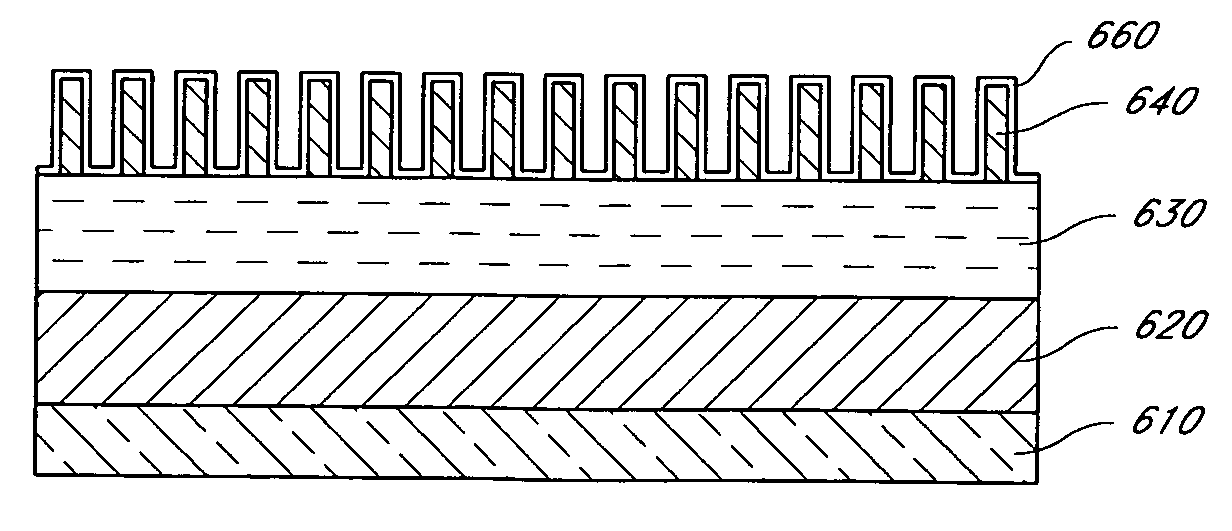
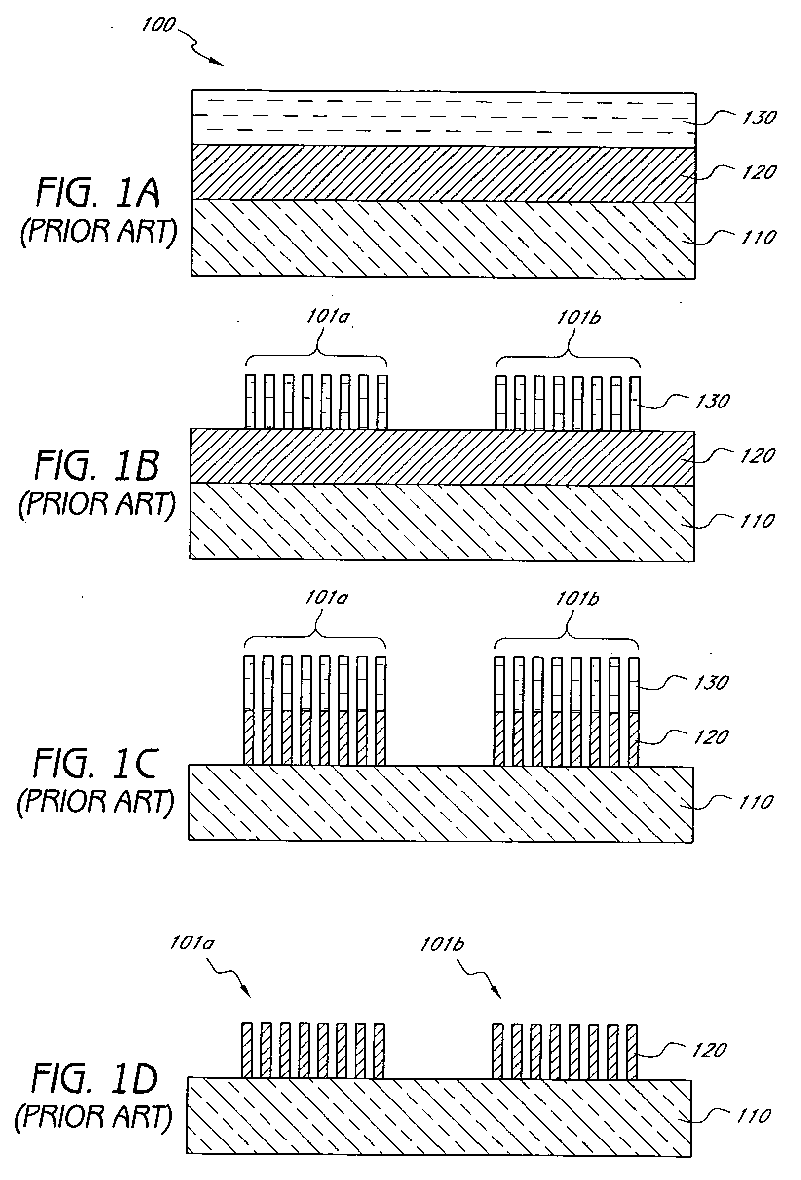
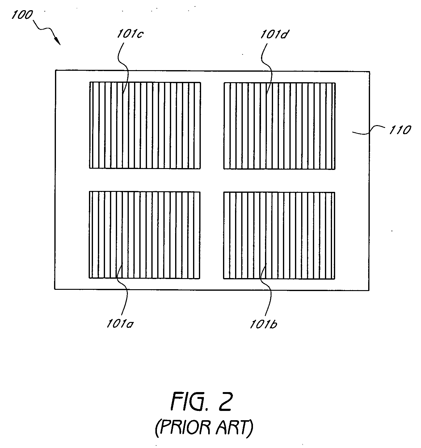
[0020] In the context of this document, the term “integrated circuit (IC) device” refers to a semiconductor device, including, but not limited to, a memory device and a microprocessor. The memory device may be volatile memories such as random access memories (RAMs) or non-volatile memories such as read-only memories (ROMs). Examples of RAMs include dynamic random access memories (DRAMs) and static random access memories (SRAMs). Examples of ROMs include programmable read-only memories (PROMs), erasable programmable read-only memories (EPROMs), electrically-erasable programmable read-only memories (EEPROMs), and flash memories.

[0021] The term “semiconductor substrate” is defined to mean any construction comprising semiconductor materials, including, but not limited to, bulk semiconductor materials such as a semiconductor wafer (either alone or in integrated assemblies comprising other materials thereon) and semiconductor material layers (either alone or in integrated as...


PUM

PropertyMeasurementUnit
Fractionaaaaaaaaaa
Fractionaaaaaaaaaa
Fractionaaaaaaaaaa

Abstract

Methods for patterning integrated circuit (IC) device arrays employing an additional mask process for improving center-to-edge CD uniformity are disclosed. In one embodiment, a repeating pattern of features is formed in a masking layer over a first region of a substrate. Then, a blocking mask is applied over the features in the masking layer. The blocking mask is configured to differentiate array regions of the first region from peripheral regions of the first region. Subsequently, the pattern of features in the array regions is transferred into the substrate. In the embodiment, an etchant can be uniformly introduced to the masking layer because there is no distinction of center/edge in the masking layer. Thus, CD uniformity can be achieved in arrays which are later defined.

Description

CROSS-REFERENCE TO RELATED APPLICATIONS [0001] This application is related to and incorporates the following by reference in their entireties: U.S. patent application Ser. No. 10 / 931,772 to Abatchev et al., filed Aug. 31, 2004; U.S. patent application Ser. No. 10 / 934,778 to Abatchev et al., filed Sep. 2, 2004; and U.S. patent application Ser. No. 11 / 214,544 to Tran et al., filed Aug. 29, 2005.BACKGROUND OF THE INVENTION [0002] 1. Field of the Invention [0003] The present invention relates to the field of integrated circuit fabrication, particularly to a process for improving critical dimension uniformity for integrated circuit arrays. [0004] 2. Description of the Related Art [0005] In the semiconductor industries, integrated circuit (IC) devices have become faster, smaller, and more efficient. This trend has continued with the development of fabrication technology to increase circuit densities on chips. [0006] Reducing critical dimension is one important way to increase circuit dens...

Claims


Application Information

Patent Timeline
IPC IPC(8): H01L21/302H01L21/461H01L29/04
CPCH01L21/0337H01L21/0338H01L27/0207H01L21/033H01L29/06H01L21/2815
Inventor KEWLEY, DAVID
Owner MICRON TECH INC
Why Eureka
Try Eureka