PEALD Deposition of a Silicon-Based Material

a technology of silicon-based materials and pealds, which is applied in the direction of chemical vapor deposition coatings, crystal growth processes, coatings, etc., can solve the problems of limiting the reaction between precursors, remains the composition of the material is therefore also relatively difficult to control, so as to improve the mobility of the transistor channel, improve the mobility of the channel, and modify the mobility of the electron or hole

Inactive Publication Date: 2007-11-01
STMICROELECTRONICS SRL
View PDF3 Cites 520 Cited by
  • Summary
  • Abstract
  • Description
  • Claims
  • Application Information

AI Technical Summary

Benefits of technology

[0016] The use of an organometallic silicon precursor allows the composition of the silicon-based material to be better controlled.
[0037] A partial purge prevents the formation of undesirable particles, while avoiding a considerable slow-down of the process.

Problems solved by technology

This is because it is relatively difficult for the TCS used as precursor in the prior art to react with ammonia, so that this reaction between the precursors constitutes a limiting step.
The plasma is applied so as to facilitate this reaction, which remains relatively tricky to control.
The composition of the material is therefore also relatively tricky to control.

Method used


Image

  • PEALD Deposition of a Silicon-Based Material
  • PEALD Deposition of a Silicon-Based Material
  • PEALD Deposition of a Silicon-Based Material

Examples


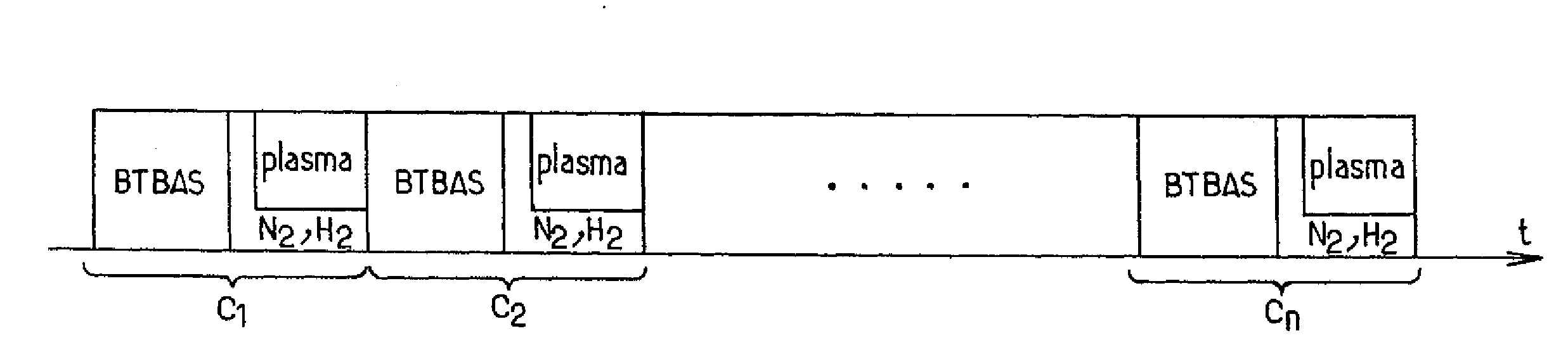
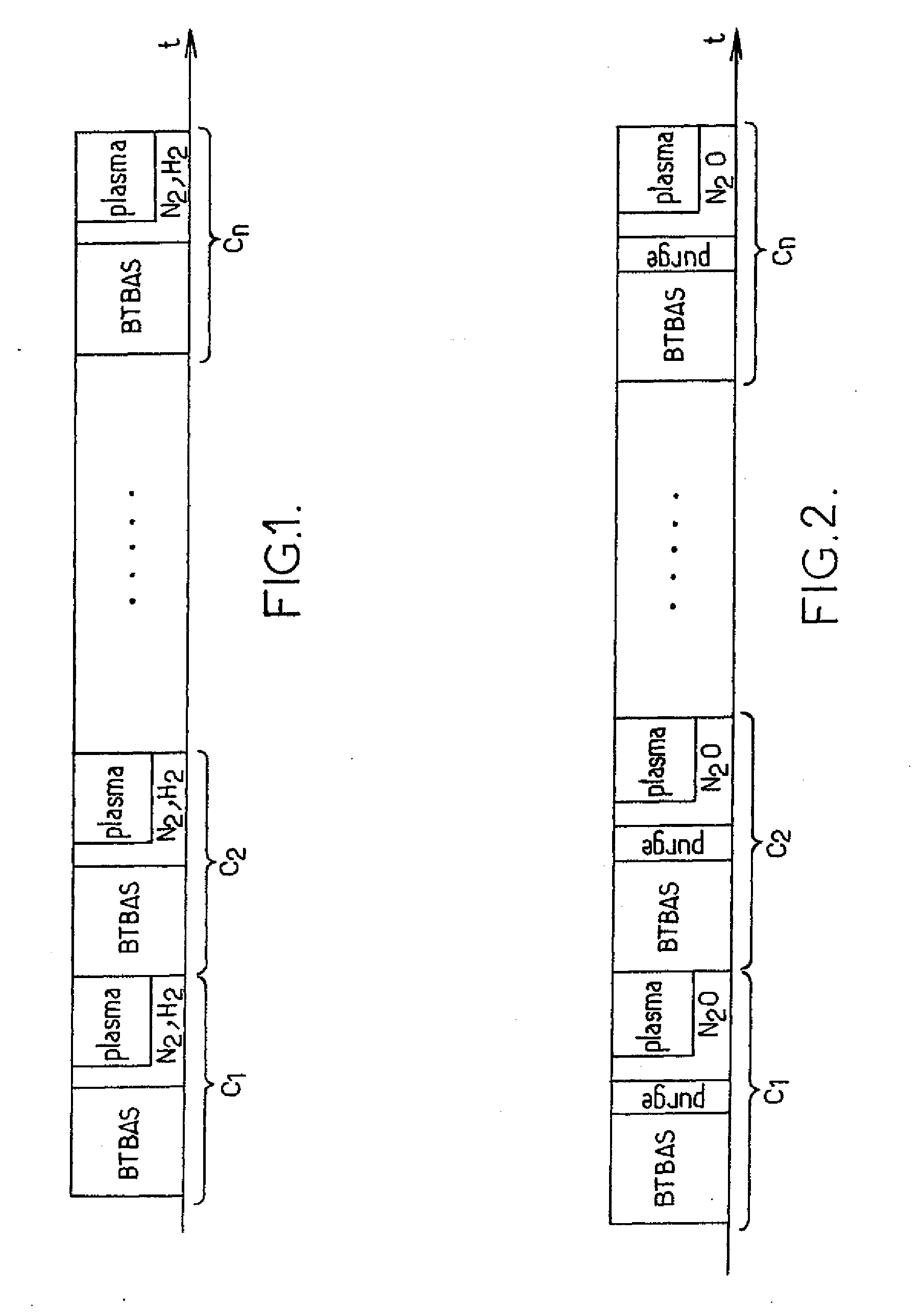
Embodiment Construction

for Obtaining Semiconductor Products

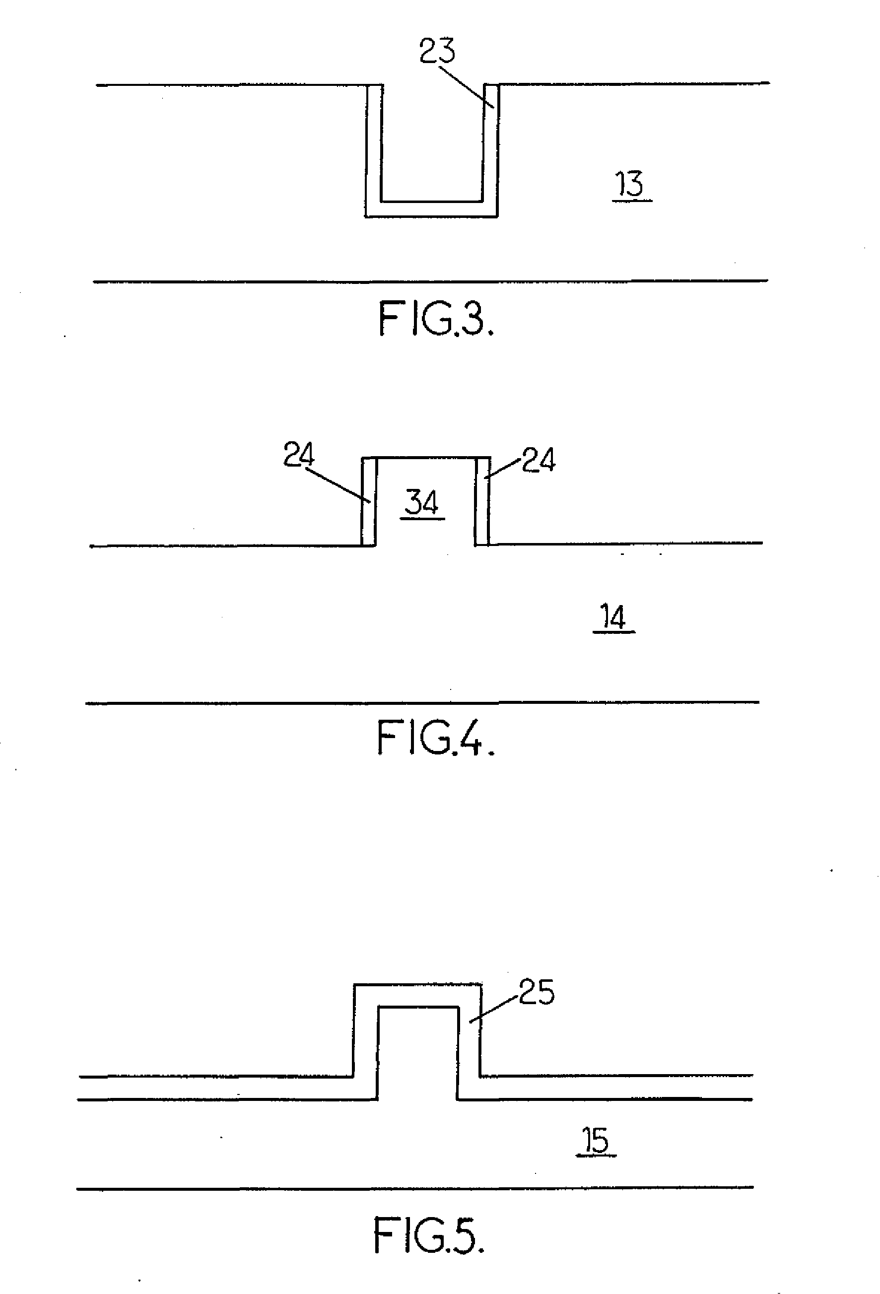
[0060]FIGS. 3, 4 and 5 show examples of semiconductor products according to embodiments of the invention.

[0061]FIG. 3 shows very schematically a 3D capacitor comprising a layer 23 made of a silicon-based material deposited on a substrate 13.

[0062] The substrate 13 comprises a layer of a dielectric material into which a trench is cut. The substrate 13 may possibly comprise other layers (not shown), for example electrodes of the capacitor 3D, and also copper interconnects (not shown), etc.

[0063] The trench may be obtained by an anisotropic etching step. After the layer made of silicon-based material has been deposited using a PEALD process according to one aspect of the invention, a polishing step of the CMP (chemical-mechanical polishing) type makes it possible to remove the layer deposited on the surface of the layer of dielectric material, so that only the internal walls of the trench are coated with the layer of silicon-based material. This l...


PUM

PropertyMeasurementUnit
temperatureaaaaaaaaaa
temperaturesaaaaaaaaaa

Abstract

A process for depositing a silicon-based material on a substrate uses the technology of plasma-enhanced atomic layer deposition. The process is carried out over several cycles, wherein each cycle includes: exposing the substrate to a first precursor, which is an organometallic silicon precursor; and applying a plasma of at least a second precursor, different from the first precursor. Semiconductor products such as 3D capacitors, vertical transistor gate spacers, and conformal transistor stressors are made from the process.

Description

PRIORITY CLAIM [0001] The present application is a translation of and claims priority from French Patent Application No. 06 03684 of the same title filed Apr. 25, 2006, the disclosure of which is hereby incorporated by reference. BACKGROUND OF THE INVENTION [0002] 1. Technical Field of the Invention [0003] The present invention relates to deposition of silicon-based material on a substrate in a process for fabricating a semiconductor product. [0004] The process is applicable in many fields. For example, the invention may be employed within the context of fabricating a three-dimensional capacitor or 3D capacitor. [0005] 2. Description of Related Art [0006] The term “substrate” is understood to mean any material on which a silicon-based material is deposited. For example, in the case of a 3D capacitor, the substrate comprises a layer of a dielectric material into which a trench is cut, and also possibly other subjacent layers, for example electrodes. [0007] The substrate may have a co...

Claims


Application Information

Patent Timeline
Patent Type & Authority Applications(United States)
IPC IPC(8): C30B23/00C30B28/14
CPCC23C16/345C23C16/401C23C16/515C23C16/45553C23C16/45542
Inventor GROS-JEAN, MICHAELBENOIT, DANIELREGOLINI, JORGE LUIS
Owner STMICROELECTRONICS SRL
Why Eureka
Try Eureka