Piezoelectric thin-film resonator and filter using the same
a thin-film filter and resonator technology, applied in piezoelectric/electrostrictive device material selection, piezoelectric/electrostrictive/magnetostrictive device material selection, device material selection, etc., can solve the problem of difficult to restrain the lateral leakage, the lateral leakage of acoustic waves cannot be easily restrained, etc. problem, to achieve the effect of reducing loss, preventing lateral leakage of acoustic waves
- Summary
- Abstract
- Description
- Claims
- Application Information
AI Technical Summary
Benefits of technology
Problems solved by technology
Method used
Image
Examples
first embodiment
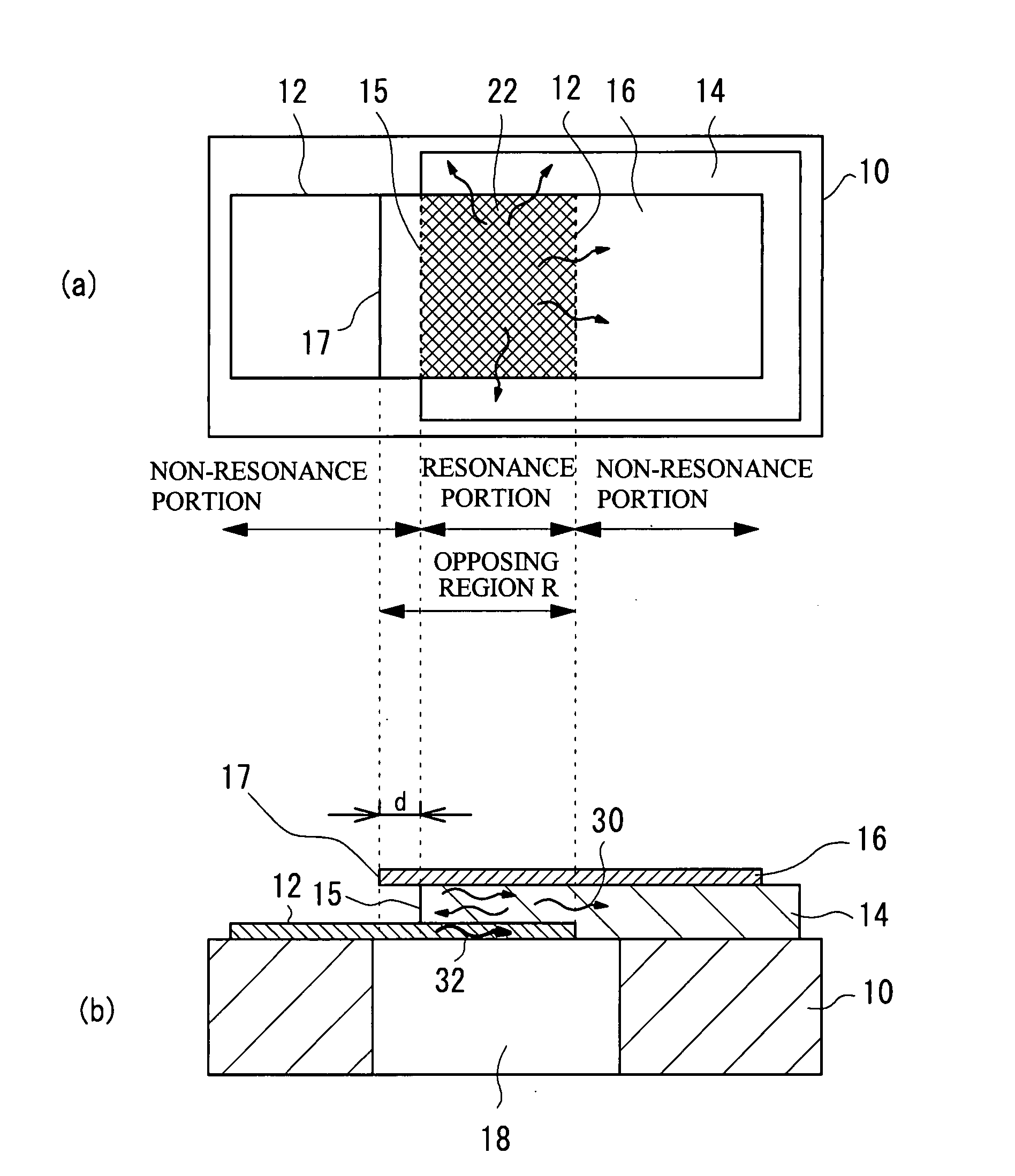
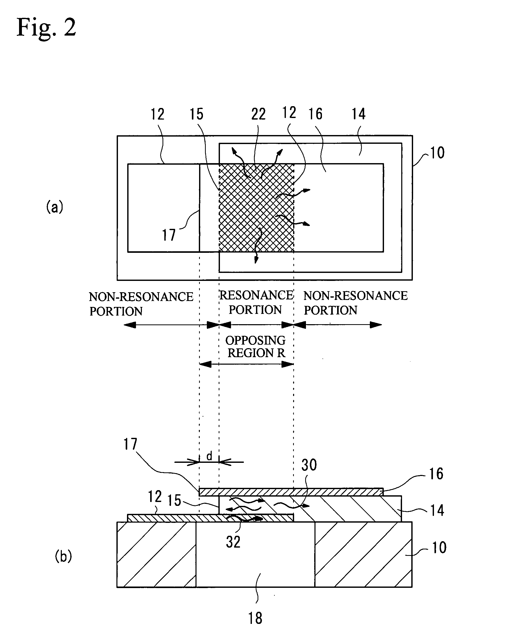
[0031]FIG. 2 shows a piezoelectric thin-film resonator in accordance with a first embodiment. More particularly, part (a) of FIG. 2 is a plan view of the resonator, and part (b) is a cross-sectional view taken along a longitudinal line in part (a).
[0032]The lower electrode 12 formed on the silicon substrate 10 has a two-layer structure composed of a Ru film and a Cr film. The piezoelectric film 14, which may be made of AlN, is provided on the lower electrode 12 and the silicon substrate 10. The upper electrode 16, which may be made of Ru, is provided so as to have the overlapping portion (resonance portion) 22 in which the upper electrode 16 overlaps the lower electrode 12 across the piezoelectric film 14. The cavity 18 is formed in the silicon substrate 10 and is located below the resonance portion 22. The cavity 18 may be an acoustic multilayer film.
[0033]At least a part of an outer end 15 of the piezoelectric film 14 in the resonance portion 22 (the left-hand side of the resonanc...
second embodiment
[0039]Referring to FIG. 6, a second embodiment is a piezoelectric thin-film resonator in which at least a part of an end surface 26 of the upper electrode 16 in the region R defined by overlapping the upper electrode 16 and the lower electrode 12 across the piezoelectric film 14 is inclined to a lower surface 25 of the upper electrode 16. Further, the piezoelectric film 14 has an end surface 24 that is inclined to the lower surface 25 of the upper electrode 16 in the electrode opposing region R. The other structures of the second embodiment are the same as those of the first embodiment. A symbol α is defined as an inner angle between the inclined end surface 26 of the upper electrode 16 and the lower surface 25 thereof. A symbol β is defined as an inner angle between the inclined end surface 24 of the piezoelectric film 14 and a lower surface 27 thereof. The symbol d is the distance between the upper end of the end surface 24 of the piezoelectric film 14 and the lower end of the end...
third embodiment
[0045]A third embodiment has an arrangement in which a part of the end surface 24 of the piezoelectric film 14 in the region R in which the upper electrode 16 and the lower electrode 12 are opposite to each other across the piezoelectric film 14 is shaped into a reverse taper. Referring to FIG. 13, the inner angle β between the end surface 24 of the piezoelectric film 14 and the lower surface 27 thereof is greater than 90°. That is, the end surface 24 of the piezoelectric film 14 is shaped into a reverse taper, which may be defined by etching with ion milling. The other structures of the third embodiments are the same as those of the second embodiment.
[0046]FIGS. 14A through 14D show the results of the computer simulation of the anti-resonance impedance Zar as a function of the distance d for four combinations of α of 35° and β of 55°, α of 35° and β of 125°, α of 90° and β of 55°, and α of 90° and β of 125°. For α of 35° or 90°, the anti-resonance impedance Zar has a small dependen...
PUM
 Abstract
Description
Claims
Application Information


