

Semiconductor device and programming method
a technology of a semiconductor device and a programming method, which is applied in the direction of static storage, digital storage, instruments, etc., can solve the problems of increasing the consumption current, and achieve the effect of shortening the pre-charge time, shortening the time required for pre-charging, and reducing the consumption power
- Summary
- Abstract
- Description
- Claims
- Application Information
AI Technical Summary
Benefits of technology
Problems solved by technology
Method used
Image

Examples
Embodiment Construction
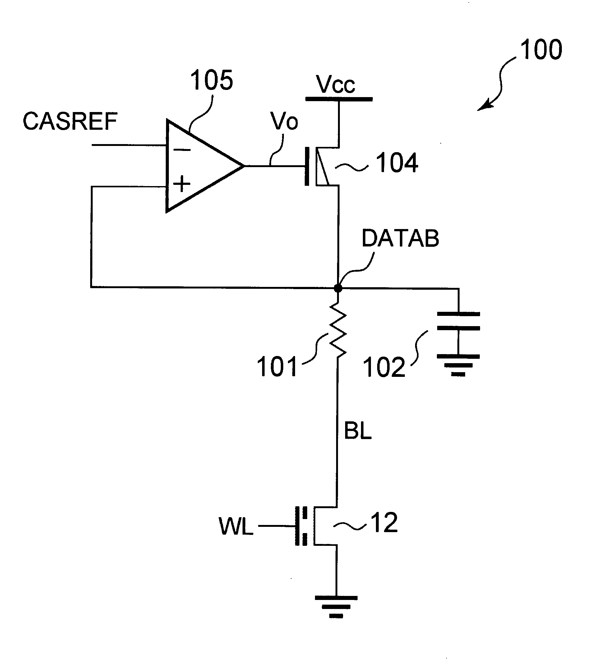
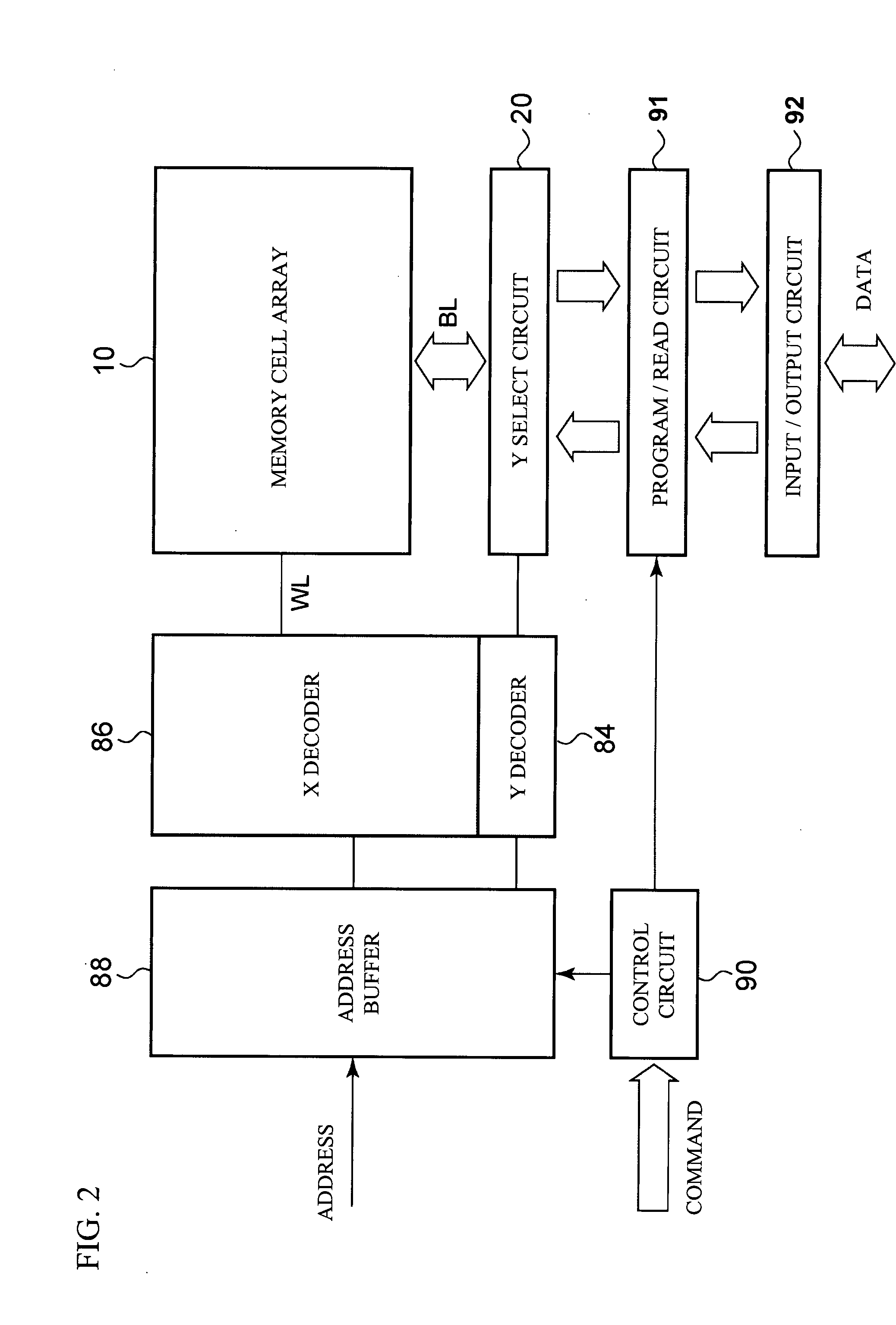
[0019] Reference will now be made in detail to the preferred embodiments of the invention, examples of which are illustrated in the accompanying drawings. While the invention will be described in conjunction with the preferred embodiments, it will be understood that they are not intended to limit the invention to these embodiments. On the contrary, the invention is intended to cover alternatives, modifications and equivalents, which may be included within the spirit and scope of the invention as defined by the claims. Furthermore, in the detailed description of the present invention, numerous specific details are set forth in order to provide a thorough understanding of the present invention. However, it will be obvious to one of ordinary skill in the art that the present invention may be practiced without these specific details. In other instances, well known methods, procedures, components, and circuits have not been described in detail as not to unnecessarily obscure aspects of t...
PUM
 Abstract
Description
Claims
Application Information