High performance stress-enhance mosfet and method of manufacture

a stress-enhanced, mosfet technology, applied in the direction of mosfet devices, basic electric elements, electrical appliances, etc., can solve the problems of general disadvantages of pfet performance and benefits of nfet performance, and achieve the effect of reducing the stress effect in the pfet channel region and higher resultant stress components

Inactive Publication Date: 2007-11-01
GLOBALFOUNDRIES US INC
View PDF99 Cites 35 Cited by
  • Summary
  • Abstract
  • Description
  • Claims
  • Application Information

AI Technical Summary

Benefits of technology

[0008] In a first aspect of the invention, a method of manufacturing a semiconductor structure includes forming, simultaneously, a layered structure with an underlying stress inducing material, in a p-type field-effect-transistor (PFET) channel region and a n-type field-effect-transistor (NFET) channel region. The method further includes protecting the NFET channel region while forming a layer over the underlying stress inducing material of the PFET channel region to reduce the stress effect in the PFET channel region. An island is etched in the NFET channel region and the PFET channel region, creating a higher resultant stress component in the NFET channel region. A stress inducing material is formed in etched portions of the PFET channel region creating an opposite stress component in the PFET channel region than in the NFET channel region.

Problems solved by technology

However, the same stress component, either tensile stress or compressive stress, discriminatively affects the characteristics of an n-type device and p-type device.
That is, because the type of stress which is beneficial for the performance of an NFET is generally disadvantageous for the performance of the PFET.
While these methods do provide structures that have tensile stresses being applied to the NFET device and compressive stresses being applied along the longitudinal direction of the PFET device, they may require additional materials and / or more complex processing and thus, resulting in higher costs.

Method used


Image

  • High performance stress-enhance mosfet and method of manufacture
  • High performance stress-enhance mosfet and method of manufacture
  • High performance stress-enhance mosfet and method of manufacture

Examples


Embodiment Construction

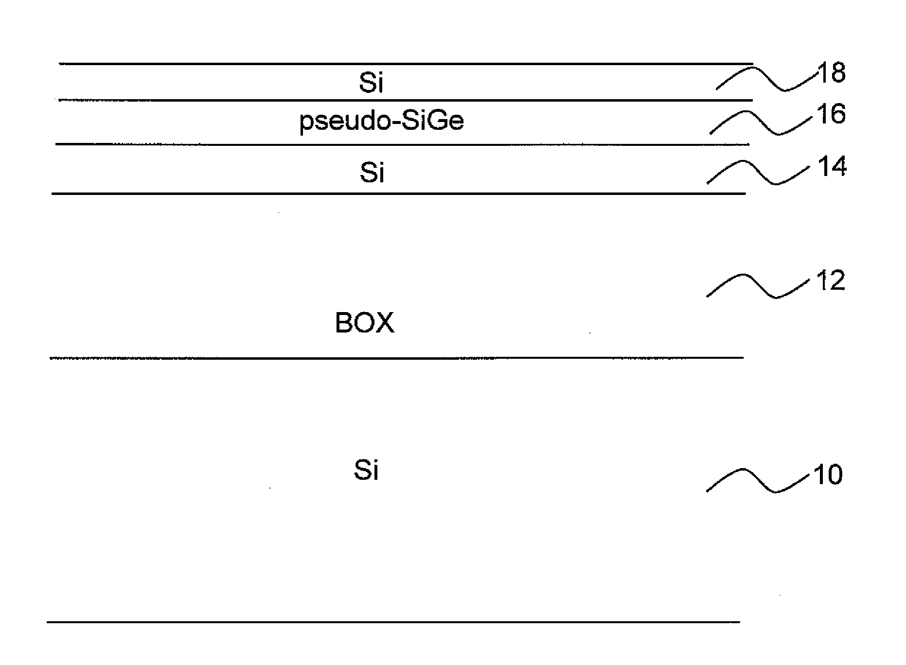
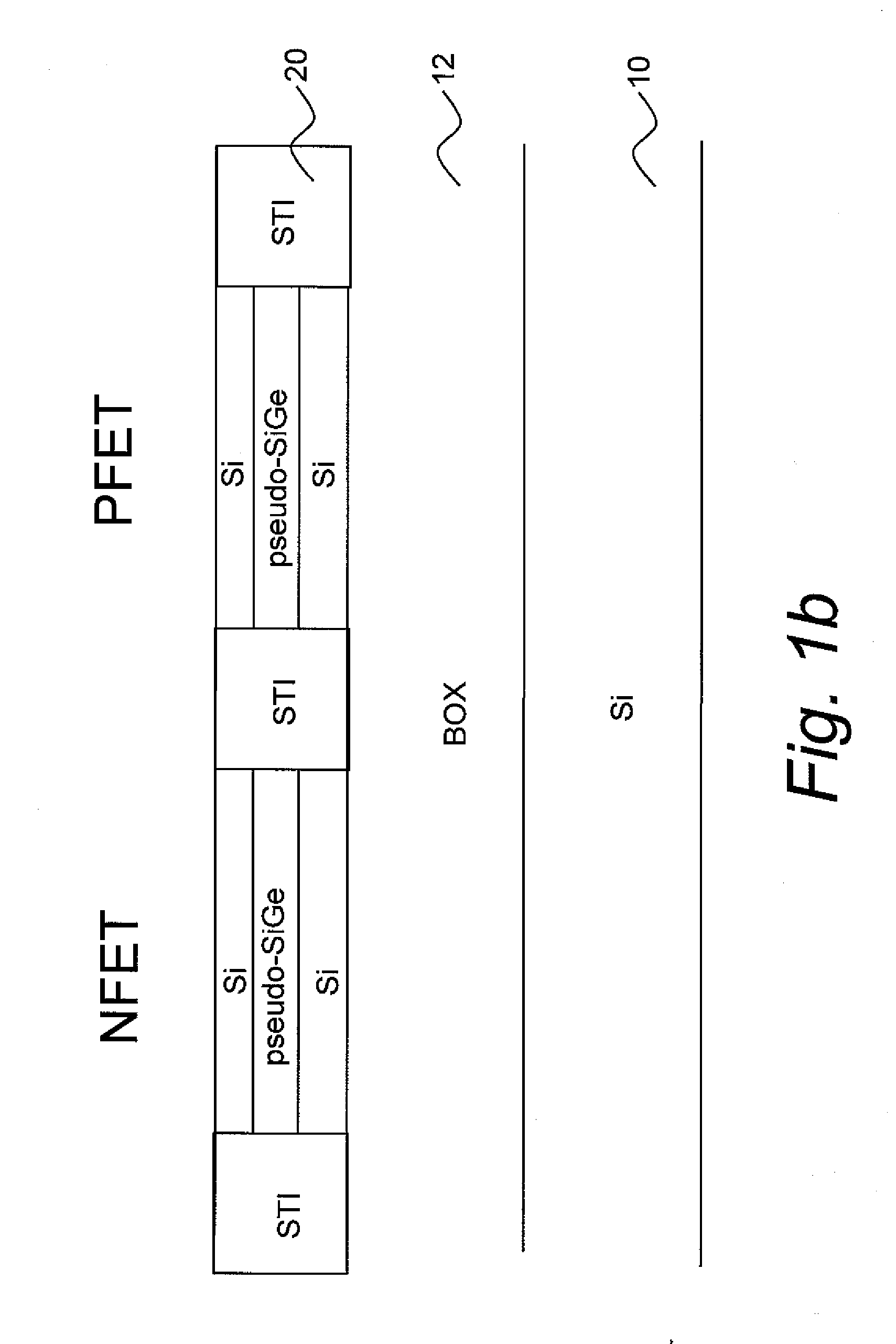
[0015] This invention is directed to a semiconductor device and method of manufacture, which provides tensile stress in the NFET channel and compressive stress in the PFET channel of the CMOS. In embodiments of the invention, the stresses formed in the NFET and PFET channel can be achieved on a same substrate using similar processing steps, thus reducing the overall material costs and time for producing such device. In embodiments, channels are formed in the silicon layer in the area of the formation of the NFETs and PFETs. The channels of the devices are then separately and selectively treated such that while one device is covered, the other device can be etched and filled to obtain desired properties. By applying these techniques, tensile or compressive forces result in the overlying epitaxially grown layers in the channels of the NFETs and PFETs, respectively. In one embodiment, the overlying silicon layer of the PFETs are allowed to grow thicker than its homologous layer of the ...


PUM


Abstract

The invention relates to a semiconductor structure and method of manufacturing and more particularly to a CMOS device with a stress inducing material embedded in both gates and also in the source/drain region of the PFET and varying thickness of the PFET and NFET channel. In one embodiment, the structure enhances the device performance by varying the thickness of the top Silicon layer respective to the NFET or the PFET.

Description

FIELD OF THE INVENTION [0001] The invention generally related to a semiconductor device and method of manufacture and, more particularly, to a semiconductor device and method of manufacture which imposes tensile and compressive stresses in the device during fabrication. BACKGROUND DESCRIPTION [0002] Mechanical stresses within a semiconductor device substrate can modulate device performance. That is, stresses within a semiconductor device are known to enhance semiconductor device characteristics. Thus, to improve the characteristics of a semiconductor device, tensile and / or compressive stresses are created in the channel of the n-type device (e.g., NFETs) and / or p-type devices (e.g., PFETs). However, the same stress component, either tensile stress or compressive stress, discriminatively affects the characteristics of an n-type device and p-type device. [0003] For example, it has been known that a device exhibits better performance characteristics when formed on a silicon layer (or c...

Claims


Application Information

Patent Timeline
Patent Type & Authority Applications(United States)
IPC IPC(8): H01L21/8234H01L21/336
CPCH01L21/823807H01L21/823814H01L27/1203H01L29/7848H01L29/6653H01L29/66636H01L29/7843H01L29/1054Y10S438/938
Inventor CHIDAMBARRAO, DURESETIDONATON, RICARDOHENSON, WILLIAMRIM, KERN
Owner GLOBALFOUNDRIES US INC
Why Eureka
Try Eureka