Modifying work function in PMOS devices by counter-doping

a work function and counter-doping technology, applied in semiconductor devices, digital storage, instruments, etc., can solve the problems of difficult improvement of drive current of pull-down nmos devices, adversely affecting device drive current, and severe degradation of carrier mobility, so as to improve write speed and reliability, and increase write margins

Inactive Publication Date: 2007-11-08
TAIWAN SEMICON MFG CO LTD
View PDF7 Cites 26 Cited by
  • Summary
  • Abstract
  • Description
  • Claims
  • Application Information

AI Technical Summary

Benefits of technology

[0014] With the counter-doping in the gate electrode of the PMOS devices, SRAM cells and inverters have increased write margins. The write speed and reliability are also improved.

Problems solved by technology

Continuing the scaling of MOSFETs results in severe degradation of carrier mobility, however, which in turn adversely affects the device drive current.
The drive currents of pull-down NMOS devices, however, are difficult to improve, and thus have relatively smaller drive currents.
The unbalanced performance of PMOS and NMOS devices causes a writing problem.
Consequently, it takes a long period of time to write the state “0” Additionally, write margins of the SRAM cells are degraded due to the high drive currents of PMOS devices.
A low write margin results in an increased possibility of erroneous writing.
The above-discussed problems have also been found in the design of inverters.
However, when technologies evolve into 65 nm or lower, there is very little room for increasing the gate lengths, and the resulting reductions in drive currents of PMOS devices are not adequate to compensate for the increase in drive currents due to the formation of SiGe stressors.
However, the leakage currents are increased with the increase in the doping concentration adjacent the channel regions.
Therefore, the ability to increase the gate lengths of PMOS devices and to increase the pocket / channel implantation dosages is limited.
Such a solution is not preferred, however, since the peripheral circuit typically occupies a small region on a memory chip, and thus SiGe stressors will only be formed in a small region, resulting in pattern loading effects and process difficulties for subsequent process steps.

Method used


Image

  • Modifying work function in PMOS devices by counter-doping
  • Modifying work function in PMOS devices by counter-doping
  • Modifying work function in PMOS devices by counter-doping

Examples


Embodiment Construction

[0020] The making and using of the presently preferred embodiments are discussed in detail below. It should be appreciated, however, that the present invention provides many applicable inventive concepts that can be embodied in a wide variety of specific contexts. The specific embodiments discussed are merely illustrative of specific ways to make and use the invention, and do not limit the scope of the invention.

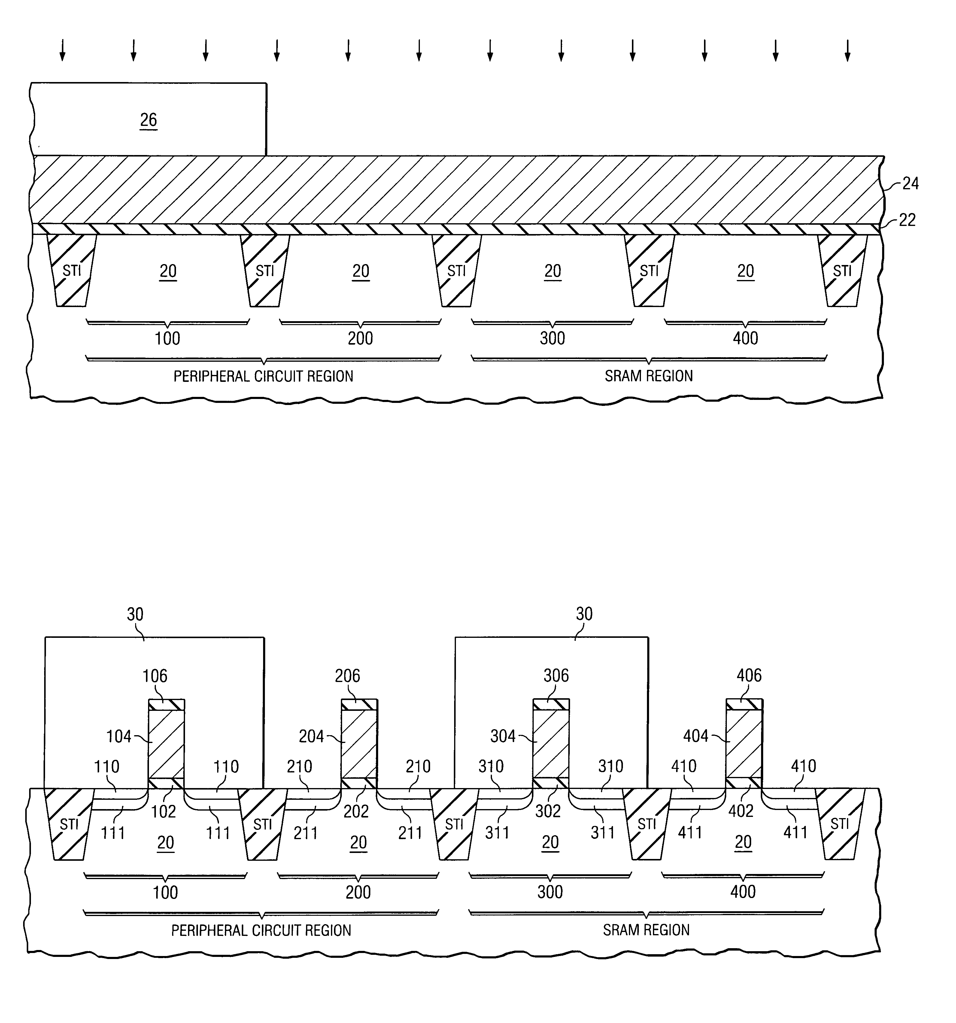
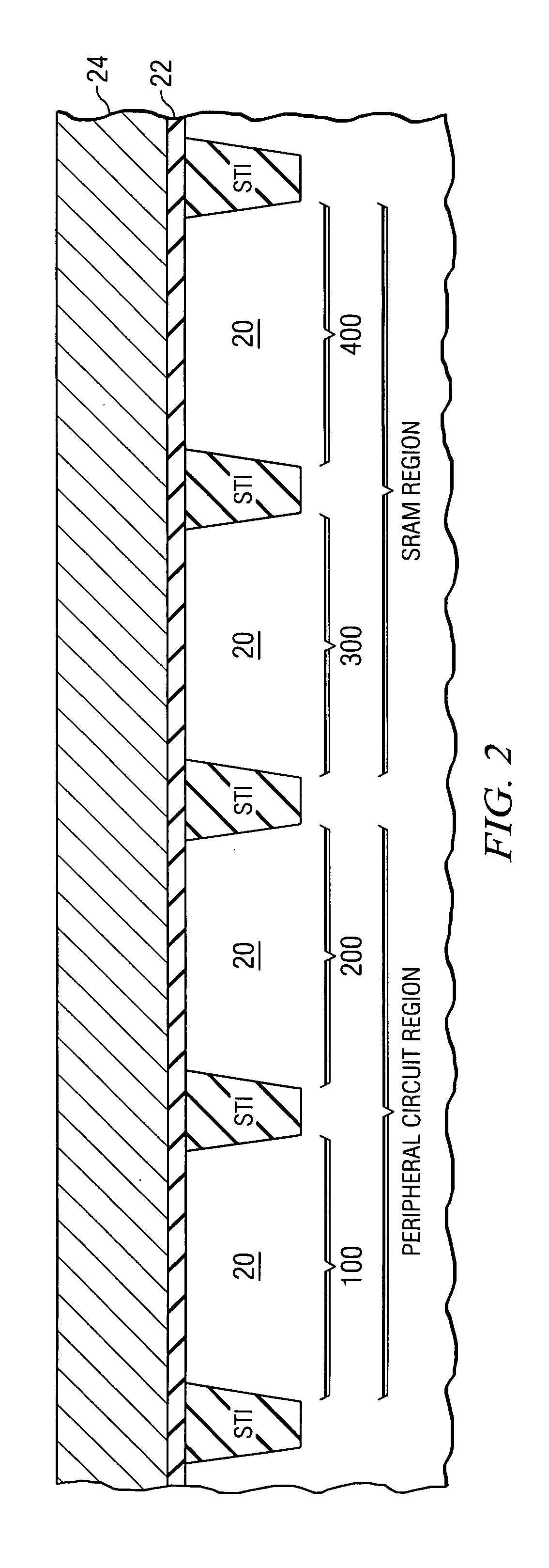
[0021] The intermediate stages of manufacturing a preferred embodiment of the present invention, which combines the formation of PMOS and NMOS devices for peripheral circuits and SRAM cells, are illustrated. Throughout the various views and illustrative embodiments of the present invention, like reference numbers are used to designate like elements. It should be appreciated that although a SRAM region is referred to (and illustrated) throughout the description for simplicity, the present invention is readily applied to the design of inverters or any other circuits preferrin...


PUM


Abstract

A semiconductor structure comprising an SRAM / inverter cell and a method for forming the same are provided, wherein the SRAM / inverter cell has an improved write margin. The SRAM / inverter cell includes a pull-up PMOS device comprising a gate dielectric over the semiconductor substrate, a gate electrode on the gate dielectric wherein the gate electrode comprises a p-type impurity and an n-type impurity, and a stressor formed in a source / drain region. The device drive current of the pull-up PMOS device is reduced due to the counter-doping of the gate electrode.

Description

TECHNICAL FIELD [0001] This invention relates generally to semiconductor devices, and more particularly to memory cells, and even more particularly to the fabrication of integrated circuits comprising static random access memory cells. BACKGROUND [0002] Scaling of semiconductor devices (e.g., a metal-oxide semiconductor field-effect transistor) has enabled continued improvement in speed, performance, density, and cost per unit function of integrated circuits over the past few decades. Continuing the scaling of MOSFETs results in severe degradation of carrier mobility, however, which in turn adversely affects the device drive current. To further enhance the performance of MOS devices, carrier mobility enhancement becomes a key element in developing next generation technologies. Among efforts to improve carrier mobility, introducing stress into the channel region of MOS devices is widely adopted. Generally, it is desirable to induce a tensile stress in the channel region of an n-type ...

Claims


Application Information

Patent Timeline
Patent Type & Authority Applications(United States)
IPC IPC(8): H01L29/76H01L29/94H01L31/00
CPCG11C11/412Y10S438/919H01L27/11H01L27/1104H01L27/1116H01L29/1083H01L29/165H01L29/6656H01L29/6659H01L29/66636H01L29/7833H01L29/7848H01L27/0883H01L27/092H01L27/105H10B10/00H10B10/12H10B10/18
Inventor LEE, CHUN-YICHUANG, HARRYWANG, PING-WEITHEI, KONG-BENG
Owner TAIWAN SEMICON MFG CO LTD
Why Eureka
Try Eureka