Electroluminescent device having improved light output

a technology of electroluminescent devices and enhancement structures, which is applied in the direction of discharge tubes/lamp details, discharge tubes luminescent screens, coatings, etc., can solve the problems of reducing the output efficiency of electroluminescent devices, the enhancement structures cannot access the air-mode light and the substrate-mode, and the enhancement structures are not very effective in enhancing the output of electroluminescent devices. , to achieve the effect of increasing the light output of an electroluminescent device and being

Active Publication Date: 2007-11-08
GLOBAL OLED TECH
View PDF21 Cites 158 Cited by
  • Summary
  • Abstract
  • Description
  • Claims
  • Application Information

AI Technical Summary

Benefits of technology

[0011] The present invention has the advantage that it increases the light output of an electrolum...

Problems solved by technology

Light trapping due to total internal reflection thus decreases drastically the output efficiency of electroluminescent devices.
These enhancement structures can only access the air-mode light and the substrate-mode light since the organic-mode of light never reaches these structures.
Since the organic-mode light constitute about half of the light generated, these enhancement structures are not very effective in enhancing the output of the electroluminescence device.
Constructing this in...

Method used


Image

  • Electroluminescent device having improved light output
  • Electroluminescent device having improved light output
  • Electroluminescent device having improved light output

Examples


Embodiment Construction

[0020] The present invention is described below with respect to OLED devices. It should be understood, however, that the same or similar can also be applied to polymer light emitting devices (PLED) and inorganic electroluminescent devices.

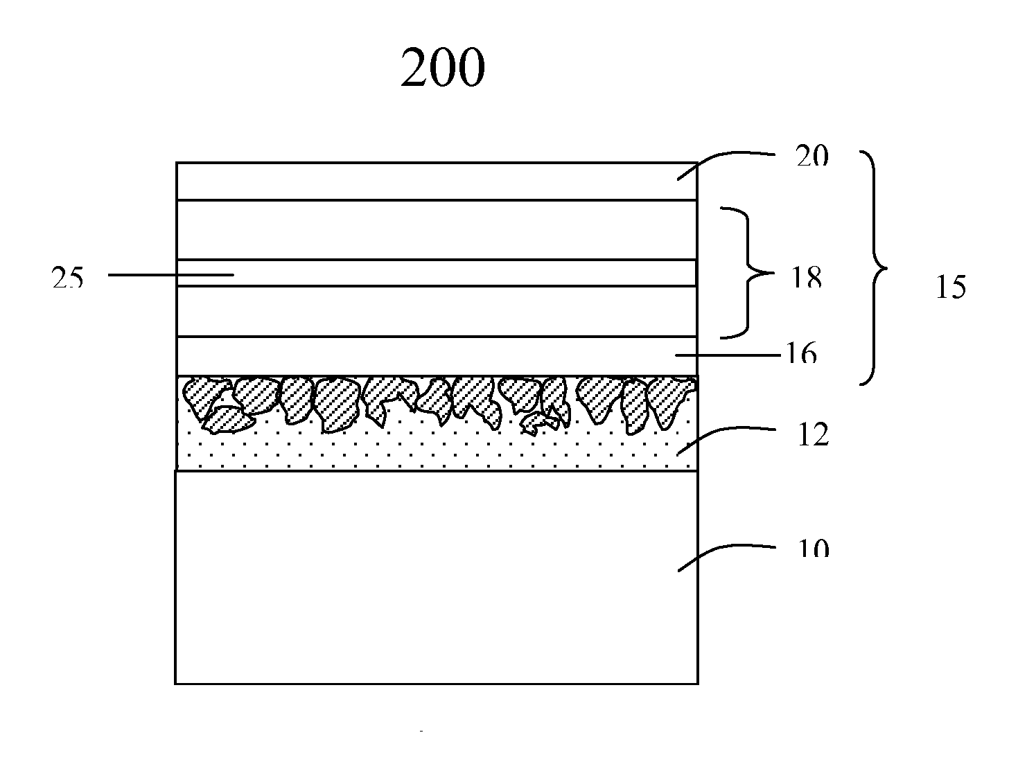
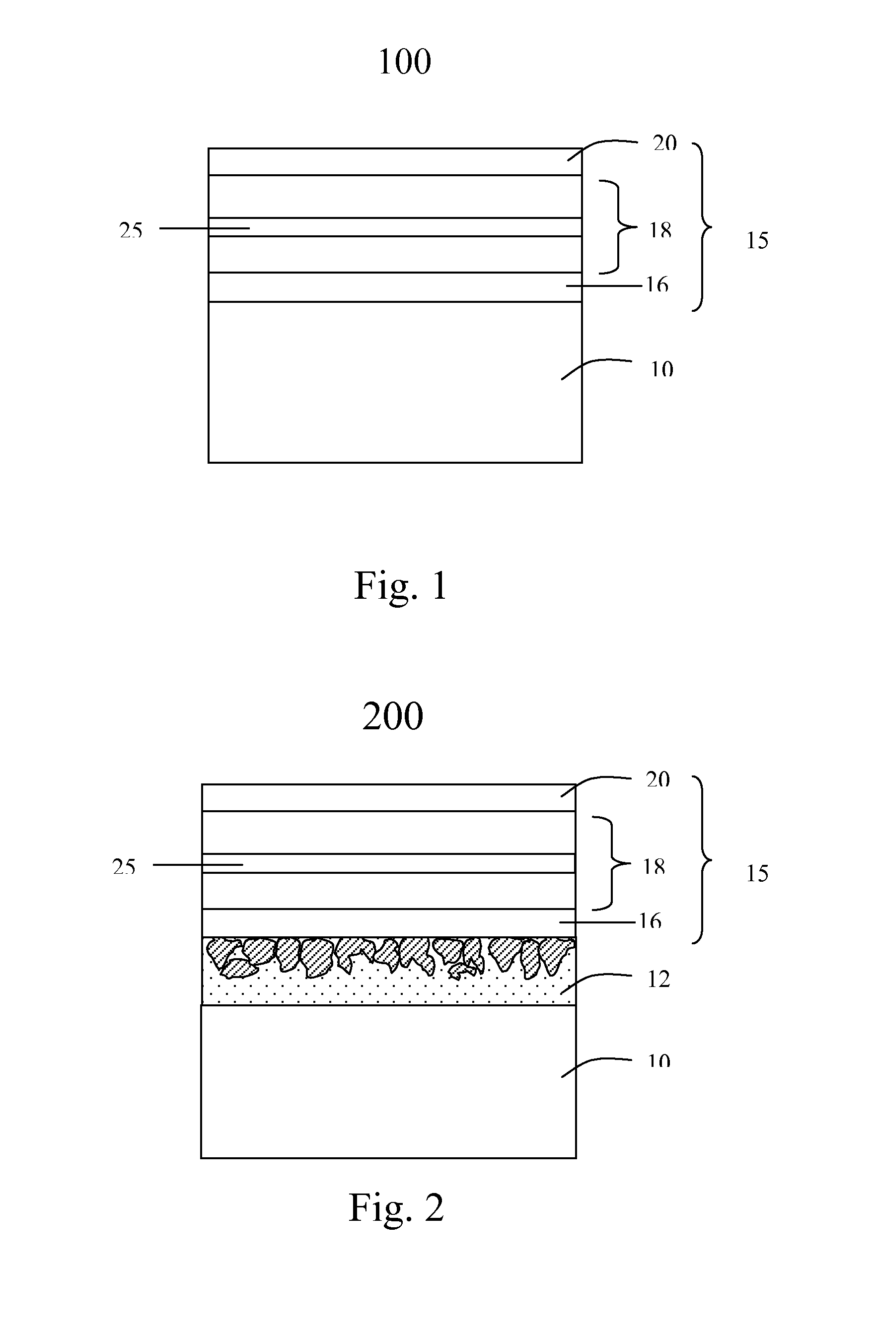
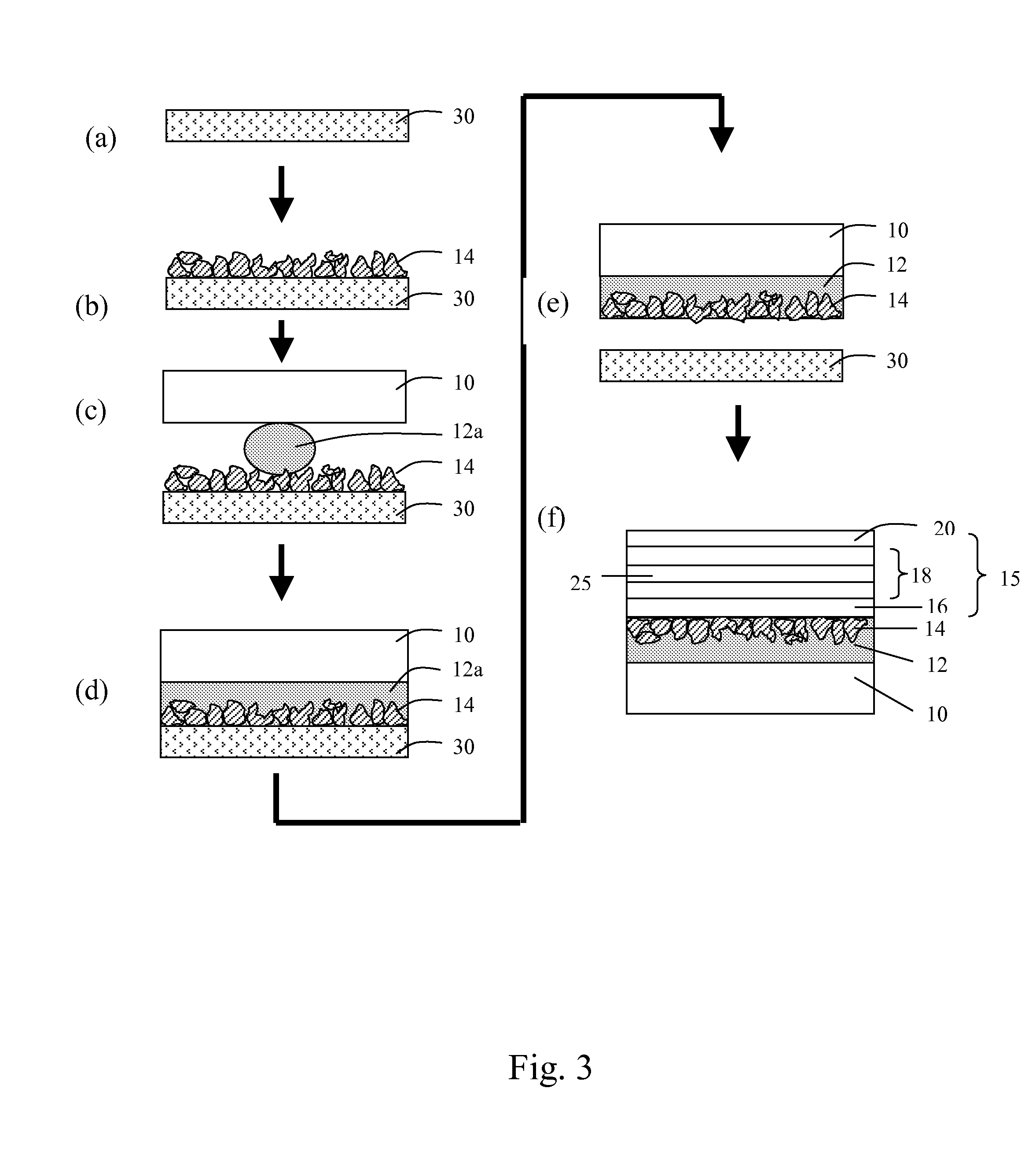
[0021] Referring to FIG. 1 there is shown a common prior art OLED device 100 as is well known in the art. OLED device 100 includes a substrate 10, an electroluminescent unit 15 including a transparent electrode layer 16, a light emitting element 18, and a reflecting electrode layer 20 in that order. Light emitting element 18 includes at least a light-emitting layer 25 and can have other layers including an electron injection layer, an electron transport layer, more light-emitting layers, a hole transport layers, and a hole injection layer. In operation a voltage is applied between transparent electrode layer 16 and reflecting electrode layer 20 causing electrical carriers to be injected into light emitting layer 25. As these carriers combine, ligh...


PUM

PropertyMeasurementUnit
Thicknessaaaaaaaaaa
Thicknessaaaaaaaaaa
Thicknessaaaaaaaaaa

Abstract

An electroluminescent device including a transparent substrate, a securing layer, a light scattering layer, an electroluminescent unit including a transparent electrode layer, a light emitting element including at least one light emitting layer, and a reflecting electrode layer in that order, wherein the light scattering layer includes one monolayer of inorganic particles having an index of refraction larger than that of the light emitting layer and wherein the securing layer holds the inorganic particles in the light scattering layer.

Description

CROSS REFERENCE TO RELATED APPLICATION [0001] Reference is made to commonly assigned U.S. patent application Ser. No. 10 / 822,517 filed Apr. 12, 2004, by Yuan-Sheng Tyan et al, entitled “OLED Device With Short Reduction” the disclosure of which is herein incorporated by reference.FIELD OF THE INVENTION [0002] The present invention relates to electroluminescent devices, and more particularly, to thin-film electroluminescent device structures for improving light output. BACKGROUND OF THE INVENTION [0003] The present invention relates to electroluminescent devices. Examples of electroluminescent devices include organic light emitting devices (OLED), polymer light emitting devices (PLED), and inorganic electroluminescent devices. [0004] A typical prior art electroluminescent device comprises a transparent substrate, a transparent first electrode layer, a light-emitting element including at least one light-emitting layer, and a reflecting second electrode layer. Light is generated in the ...

Claims


Application Information

Patent Timeline
IPC IPC(8): H05B33/00
CPCC03C17/38C03C2217/48H01L51/5268C03C2217/948C03C2217/944H10K50/854
Inventor TYAN, YUAN-SHENGWANG, JIN-SHANKESEL, RAYMOND A.FARRUGGIA, GIUSEPPECUSHMAN, THOMAS R.
Owner GLOBAL OLED TECH
Why Eureka
Try Eureka