E-fuse and method for fabricating e-fuses integrating polysilicon resistor masks

a technology of polysilicon resistor and e-fuses, which is applied in the direction of semiconductor devices, semiconductor/solid-state device details, electrical apparatus, etc., can solve the problems of negative affecting product reliability and yield, and achieve the effect of preventing current flow and lowering series resistan

Inactive Publication Date: 2007-11-15
IBM CORP
View PDF8 Cites 18 Cited by
  • Summary
  • Abstract
  • Description
  • Claims
  • Application Information

AI Technical Summary

Benefits of technology

[0012] Principal aspects of the present invention are to provide an E-fuse and a method for fabricating the E-fuse integrating polysilicon resistor masks. Other important aspects of the present invention are to provide such E-fuse and method for fabricating substantially without negative effect and that overcome many of the disadvantages of prior art arrangements.
[0013] In brief, an E-fuse and a method for fabricating an E-fuse are provided integrating polysilicon resistor masks. The E-fuse includes a polysilicon layer defining a fuse shape including a cathode, an anode, and a fuse neck connected between the cathode and the anode silicide formation. A silicide formation is formed on the polysilicon layer with an unsilicided portion extending over a portion of the cathode adjacent the fuse neck. The unsilicided portion substantially prevents current flow in the silicide formation region of the cathode, with electromigration occurring in the fuse neck during fuse programming.
[0014] In accordance with features of the invention, the unsilicided portion has a substantially lower series resistance than the series resistance of the fuse neck. The unsilicided portion has a defined size for providing a predefined series resistance of the unsilicided portion, whereby electromigration of the silicide layer occurs in the fuse neck and electromigration of the silicide layer is avoided in the cathode when a programming potential is applied across the silicide formation.

Problems solved by technology

This post-blow fuse resistance lowers the margin of the sensing circuit and thus negatively affects product reliability and yield.

Method used


Image

  • E-fuse and method for fabricating e-fuses integrating polysilicon resistor masks
  • E-fuse and method for fabricating e-fuses integrating polysilicon resistor masks
  • E-fuse and method for fabricating e-fuses integrating polysilicon resistor masks

Examples


Embodiment Construction

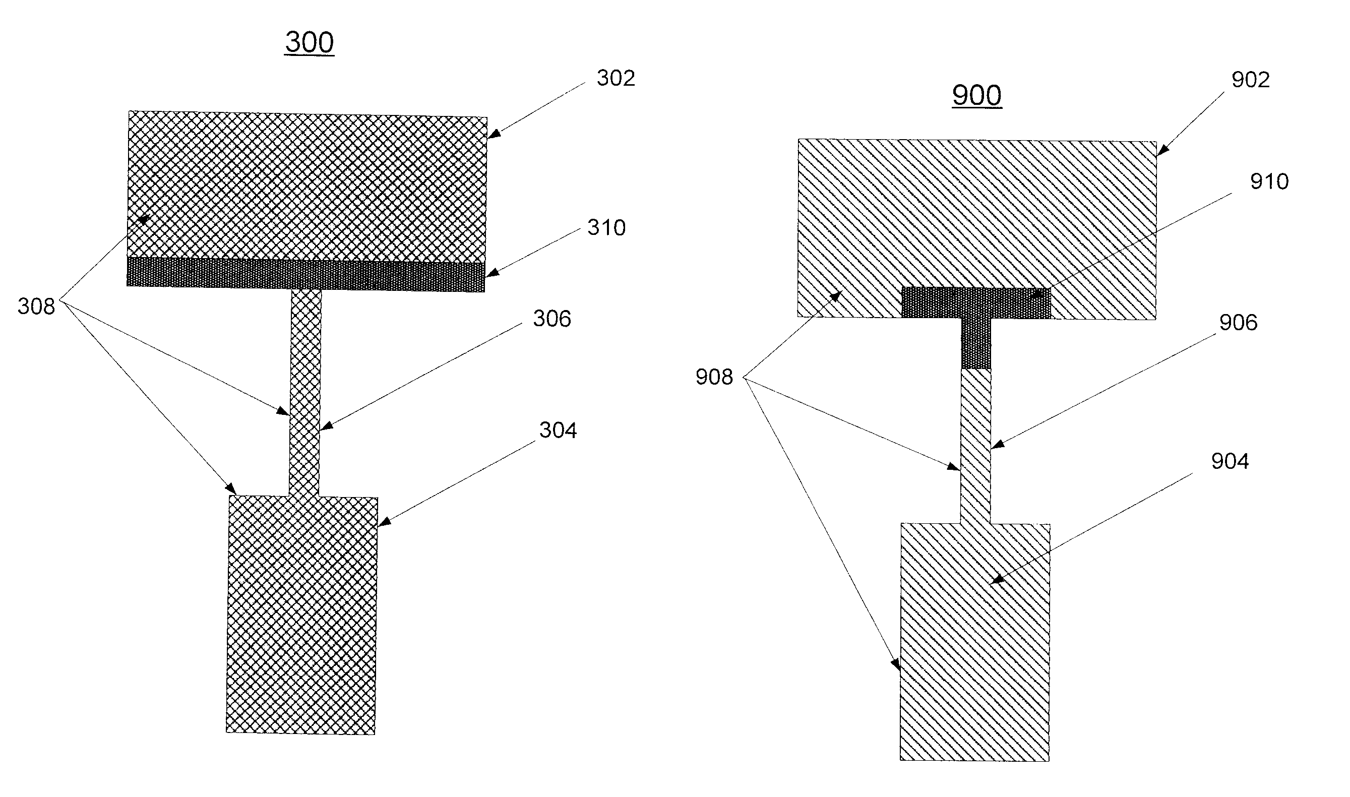
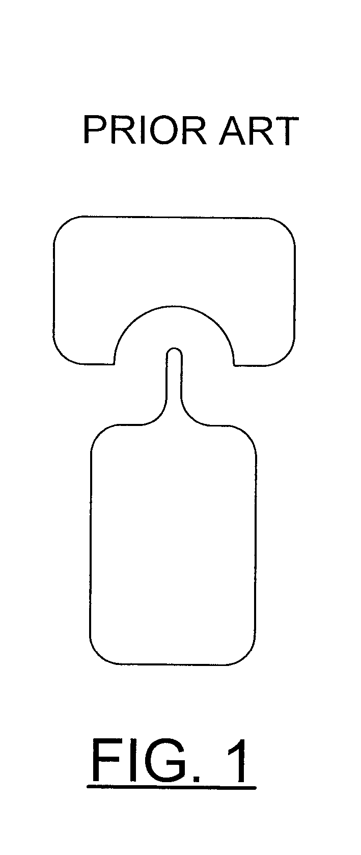
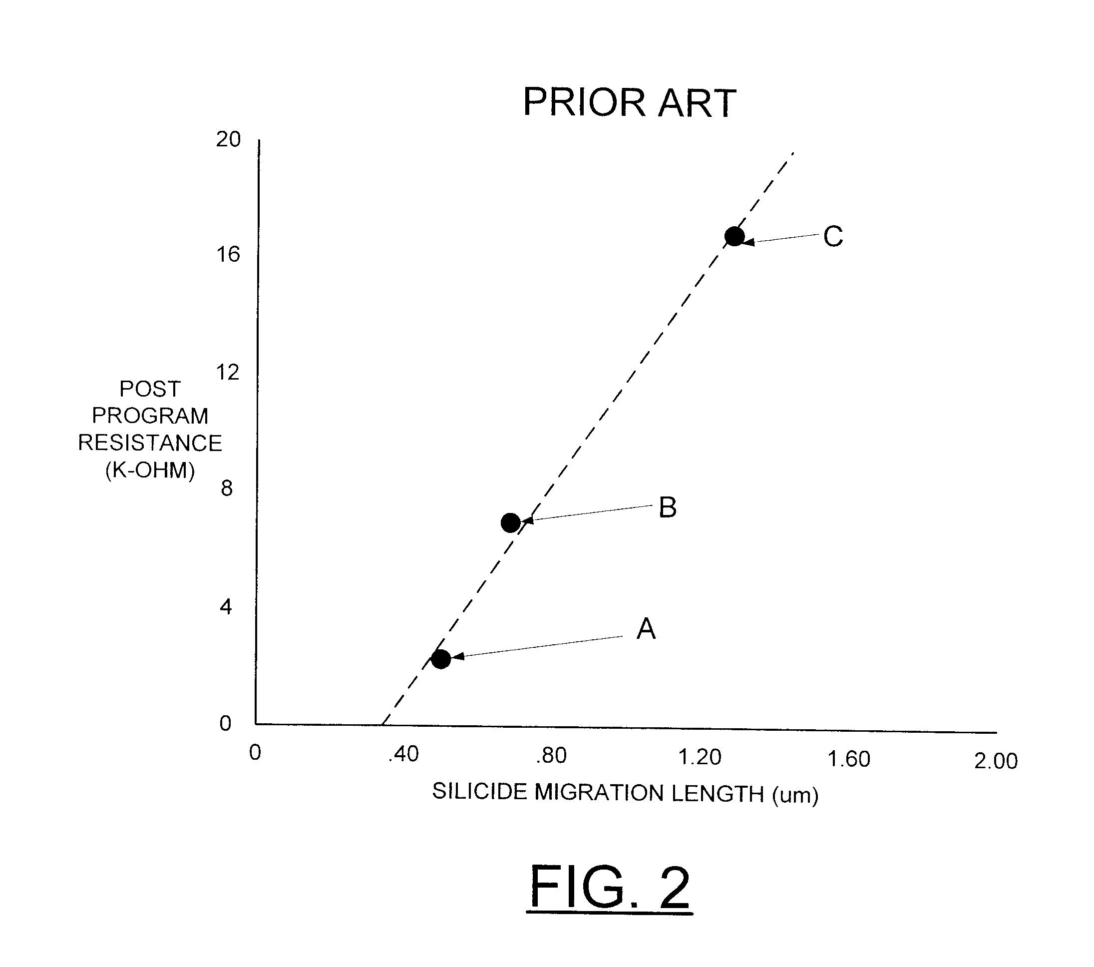
[0022] In accordance with features of the preferred embodiments, E-fuses are provided that eliminate low post-programmed fuse resistance caused by EM in the cathode rather than in the neck of the fuse element of prior art E-fuse designs, such as illustrated in FIG. 1. E-fuses of the preferred embodiments are fabricated by integrating polysilicon resistor masks without adding additional masks to the process. E-fuses of the preferred embodiments are fabricated using poly-resistor silicide-blocking and implant masks.

[0023] In accordance with features of the preferred embodiments, E-fuses are provided that do not to add any additional masks to a resistor processing sequence, for example, for CMOS technology.

[0024] In accordance with features of the preferred embodiments, the fabrication process for the E-fuses of the preferred embodiments use poly-resistor silicide-blocking and implant masks that are used in known CMOS technology, so E-fuses of the preferred embodiments advantageously...


PUM


Abstract

An E-fuse and a method for fabricating an E-fuse are provided integrating polysilicon resistor masks. The E-fuse includes a polysilicon layer defining a fuse shape including a cathode, an anode, and a fuse neck connected between the cathode and the anode silicide formation. A silicide formation is formed on the polysilicon layer with an unsilicided portion extending over a portion of the cathode adjacent the fuse neck. The unsilicided portion substantially prevents current flow in the silicide formation region of the cathode, with electromigration occurring in the fuse neck during fuse programming. The unsilicided portion has a substantially lower series resistance than the series resistance of the fuse neck.

Description

FIELD OF THE INVENTION [0001] The present invention relates generally to the field of manufacturing semiconductor devices, and more particularly, relates to an E-fuse and a method for fabricating the E-fuse integrating polysilicon resistor masks for improved fuse performance. DESCRIPTION OF THE RELATED ART [0002] Various semiconductor fuse arrangements and methods are known for fabricating semiconductor fuses and E-fuse elements. [0003] For example, U.S. Pat. No. 6,624,499 discloses a method of programming via electromigration. A semiconductor fuse, which includes a cathode and an anode coupled by a fuse link having an electrically conductive component, such as silicide, is coupled to a power supply. A potential is applied across the conductive fuse link via the cathode and anode in which the potential is of a magnitude to initiate electromigration of silicide from a region of the semiconductor fuse reducing the conductivity of the fuse link. The electromigration is enhanced by effe...

Claims


Application Information

Patent Timeline
Patent Type & Authority Applications(United States)
IPC IPC(8): H01L29/00
CPCH01L23/5256H01L2924/0002H01L2924/00
Inventor BOOTH, ROGER ALLEN JR.HOVIS, WILLIAM PAULMANDELMAN, JACK ALLANTONTI, WILLIAM ROBERT
Owner IBM CORP
Why Eureka
Try Eureka