Heat sink electronic package having compliant pedestal

Active Publication Date: 2007-11-22
DELPHI TECH IP LTD
View PDF15 Cites 81 Cited by
  • Summary
  • Abstract
  • Description
  • Claims
  • Application Information

AI Technical Summary

Problems solved by technology

Excessive heat in electronic devices and other components within an electronic package may lead to adverse effects including electrical circuit failure.
Because of various tolerance issues and since there generally is no compliance built into the packaging, an inconsistent bond-line typically exists between the semiconductor IC devices and the rigid heat sink pedestals.
The tolerance stack-ups of the various electronic devices makes it difficult to maintain a consistent thin thermal joint between the back side of the IC devices and the respective pedestals on the heat sink co

Method used


Image

  • Heat sink electronic package having compliant pedestal
  • Heat sink electronic package having compliant pedestal
  • Heat sink electronic package having compliant pedestal

Examples


first embodiment

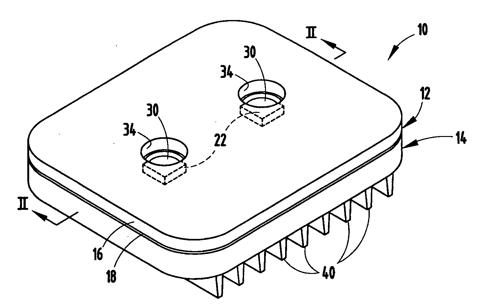
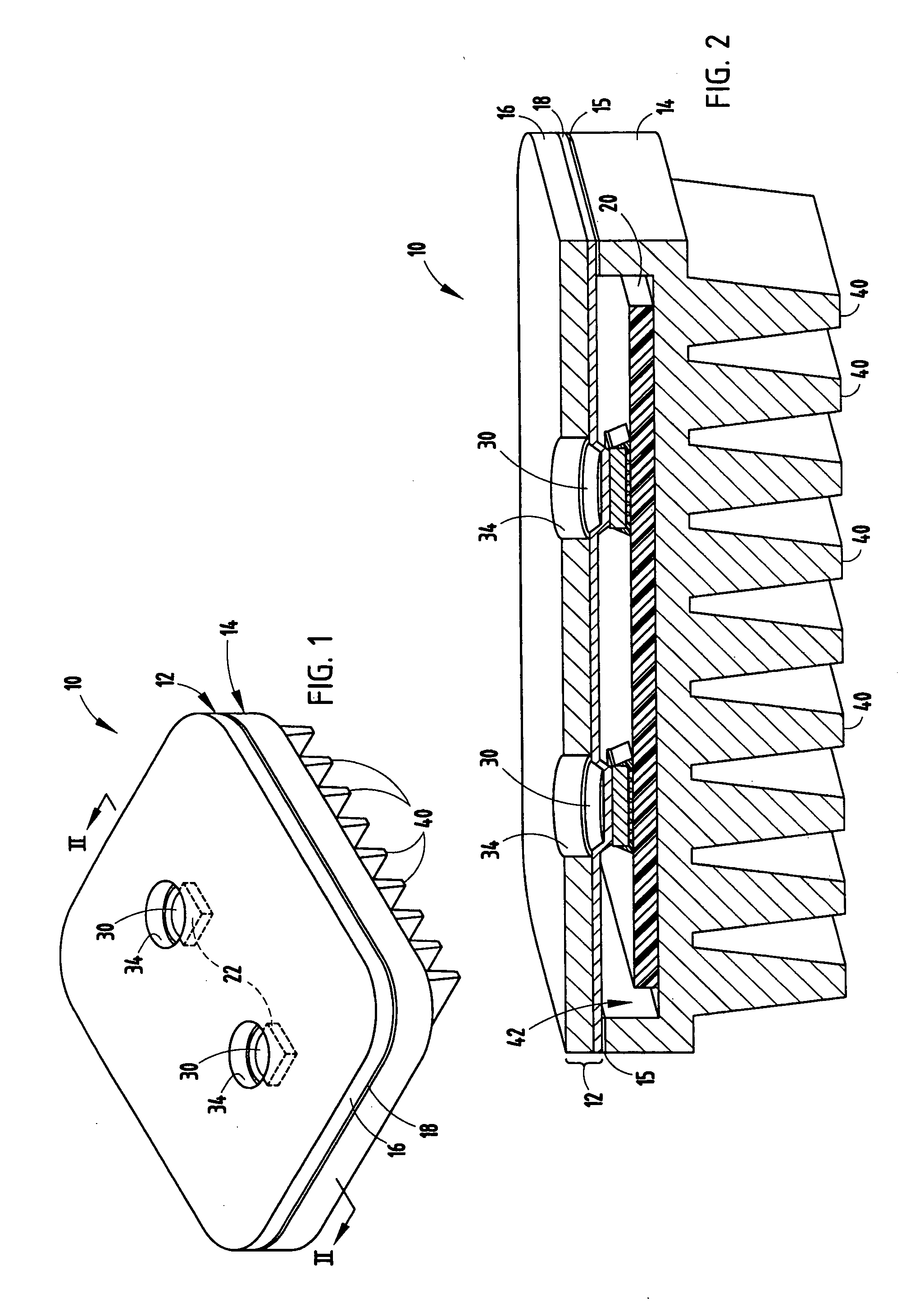
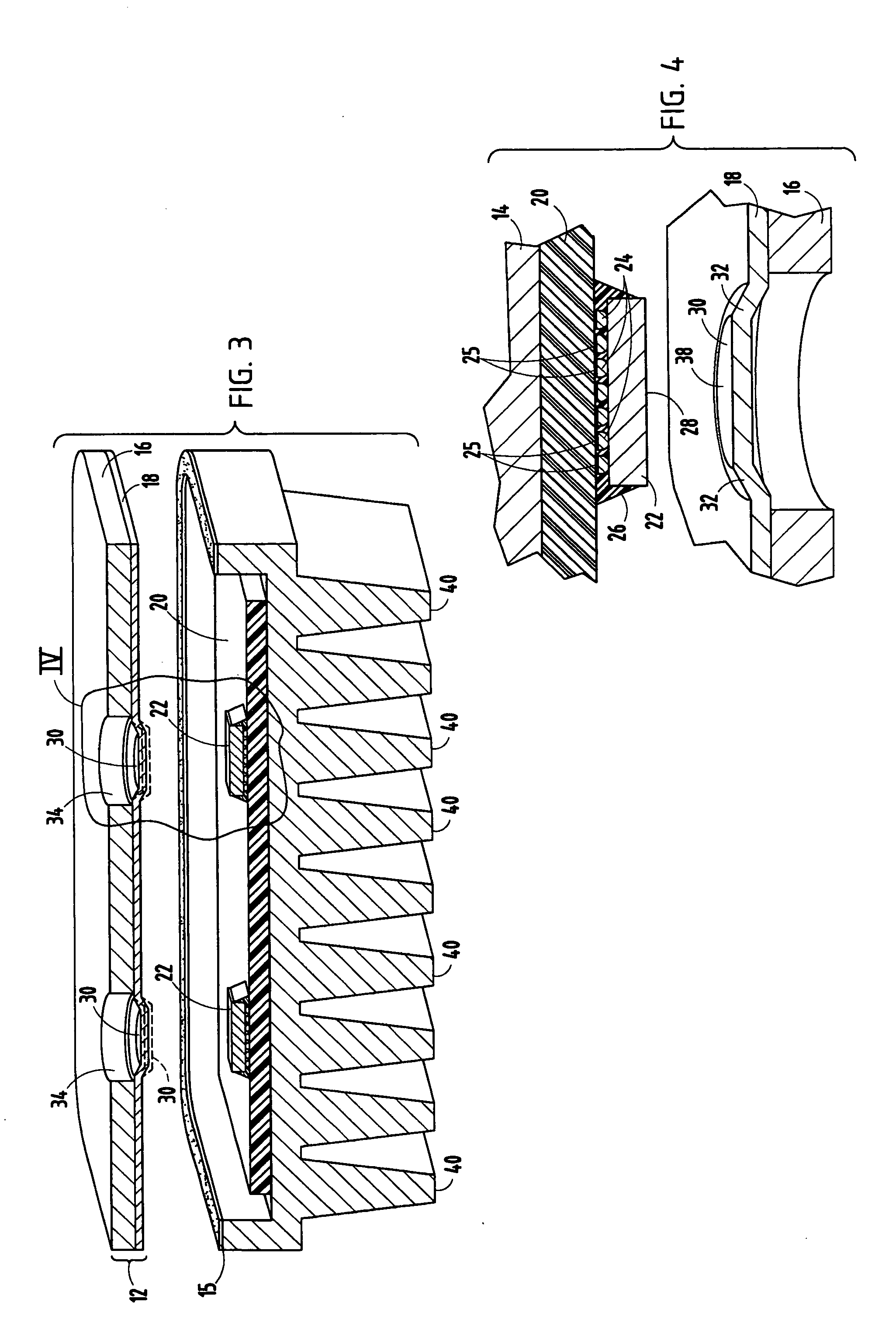
[0025]Disposed in direct contact and thermal heat transfer relationship with the upper surface of the electronic devices 22 is the heat sink upper housing member 12. the upper housing member 12 employs a stamped aluminum sheet 16 having openings 34 punched or drilled therein, and a lower sheet of copper cladding 18 formed on the bottom surface. The copper cladding 18 is then shaped to form the compliant pedestals 30. The formation of the compliant pedestals 30 may be achieved by stamping copper cladding layer 18 with a press extending through the holes 34 in aluminum layer 16 to form thin protruding pedestals 30 as locations that will align with corresponding electronic devices 22.

[0026]As seen in FIG. 4, each compliant pedestal 30 has thin angled (tapered) wall 32 that lead to a flat bottom end contact surface 38 that conforms to the like-shaped flat top surface of an electronic device 22. The contact surface 38 is intended to contact the top surface of a corresponding electronic ...

second embodiment

[0029]Referring to FIG. 5, a compliant pedestal 30′ is shown formed in upper housing heat sink member 12 having a single layer of aluminum. According to this embodiment, each compliant pedestal 30′ is formed by mechanically stamping to form the recessed pedestal 30′ and milling a reduced thickness groove 50 in an area surrounding the pedestal 30′ to form a metal spring-like structure in the upper housing. The reduced thickness groove 50 may be formed such that the thinned portion 52 of the cover has a thickness of about 5-20 mils according to one example. The ring-shaped reduced thickness groove 50 formed by milling in the upper housing member 12 is sufficiently thin to provide the desired spring rate to apply compressive force at a desired rate to the top surface of the electronic device 22 to maintain sufficient thermal contact therewith. By maintaining sufficient thermal contact between the compressive pedestal 30′ and the top of the electronic device 22, enhanced thermal energy...

third embodiment

[0030]Referring toFIG. 6, an electronic package 10 is shown employing a compliant pedestal 30″, according to the present invention. In this embodiment, the upper housing member 12 is stamped to form a protruding pedestal 30″, and a ring-shaped reduced thickness groove 60 surrounding the pedestal 30″ is milled at an angle to provide a desired spring rate. The reduced thickness groove 60 may be formed such that thinned portion 62 of the cover has a thickness of about 5-20 mils, according to one example.

[0031]Additionally, an overmolding material 70 is disposed between the upper housing member 12 and the bottom housing member 14. The overmolding material 70 operates as the holder to secure the upper and lower housing members 12 and 14 together and to hold the upper heat sink member 12 in thermal contact with the electronic device 22. According to one exemplary embodiment, the overmolding material may be an epoxy mold compound such as thermoset materials commercially available as Cookso...


PUM


Abstract

An electronic package is provided for dissipating heat away from electronic devices. The package includes a substrate and electronic devices mounted on the substrate. The package also has a thermally conductive heat sink assembled over the electronic device. The heat sink includes compliant pedestals each having a contact surface for contacting a surface of an electronic device to conduct thermal energy away from the electronic device. The package is held together such that the heat sink is in contact with the surface of an electronic device such that each compliant pedestal applies a compressive force to the surface of the electronic device.

Description

TECHNICAL FIELD[0001]The present invention generally relates to electronic packages and, more particularly, relates to a semiconductor electronic package having a heat sink assembly for dissipating heat away from the semiconductor device(s).BACKGROUND OF THE INVENTION[0002]Electronic packages, such as electronic control modules, generally contain electronic devices, such as surface mount components, typically having fabricated electrical integrated circuitry (IC). The circuitry conducts electrical current which, in turn, generates thermal energy (i.e. heat) within the electronic package. The heat may build-up to an elevated temperature within the package. Excessive heat in electronic devices and other components within an electronic package may lead to adverse effects including electrical circuit failure. Thus, it is desirable to dissipate heat away from some electronic packages.[0003]Many electronic packages employ semiconductor devices in the form of surface mount components solde...

Claims


Application Information

Patent Timeline
IPC IPC(8): H05K7/20
CPCH01L21/563H01L23/3675H01L2924/1305H01L2224/73253H01L2224/73204H01L2224/32225H01L2224/16225H01L24/72H01L25/0655H01L25/072H01L2924/01013H01L2924/01027H01L2924/01029H01L2924/01033H01L2924/01082H01L2924/01322H01L2924/09701H01L2924/13055H01L2924/14H01L2924/1433H01L2924/00012H01L2924/00H01L2924/181
Inventor BRANDENBURG, SCOTT D.CHENGALVA, SURESH K.ZIMMERMAN, DAVID W.
Owner DELPHI TECH IP LTD
Why Eureka
Try Eureka