Light-Emitting Device Manufacturing Method and Light-Emitting Device

a technology of light-emitting devices and manufacturing methods, which is applied in the direction of semiconductor lasers, semiconductor/solid-state device details, semiconductor laser structure details, etc., can solve the problems of light-emitting efficiency sometimes being lowered, light-emitting layer damage, etc., to reduce the amount of joining materials, reduce the spread of joining materials, and efficiently exhaust air or gas presen

Inactive Publication Date: 2007-12-06
STANLEY ELECTRIC CO LTD +1
View PDF2 Cites 46 Cited by
  • Summary
  • Abstract
  • Description
  • Claims
  • Application Information

AI Technical Summary

Benefits of technology

[0021] In the case of connecting the first electrode and the first lead by using the joining material, if the connecting surface of the first lead is flat, the melted or softened joining material spreads out outside a joining area wherein the first electrode is placed, because load is applied and/or minute vibration is added while the joining material is in molten or softened state. Therefore, a pattern with grooves having a plurality of cross-points or with a concave portion having a plurality of insular protrusions, is formed in advance on the element mounting part of the first lead, as a pattern to reduce spreading of the joining material. By the above method, it is possible to reduce amount of the joining material spreading out outside of the joining area, because the joining material spreading out outside the joining area, flows into the grooves or the concave portion.
[0022] In the case of forming the grooves on the element mounting part of the first lead, the grooves extending from the inside to the outside of the joining area wherein the first electrode is placed, are formed. By the above method, when the molten or softened joining material flows into the grooves, it is possible to efficiently exhaust air or gas present in the grooves, and to prevent air bubbles or cavities from remaining in the grooves of the joining area. Therefore, deterioration of joining strength, thermal conductivity and electric conductivity can be reduced. If pluralities of grooves are formed in crossing way, the joining material collides mutually at the cross-points, when the joining material, flowing into the grooves, spreads outward, and the joining material flowing outward, is restricted. As examples of such grooves, for example, grid-like grooves, a mixed pattern of radiating grooves and annular grooves, and the like are included.
[0023] When a concave portion, having a plurality of insular protrusion portions, is formed on the element mounting part of the first lead, a concave portion is formed so that the entire p

Problems solved by technology

Therefore, if a light-emitting layer is located just under an electrode to be connected by the bonding wire, the light-em

Method used


Image

  • Light-Emitting Device Manufacturing Method and Light-Emitting Device
  • Light-Emitting Device Manufacturing Method and Light-Emitting Device
  • Light-Emitting Device Manufacturing Method and Light-Emitting Device

Examples


embodiments

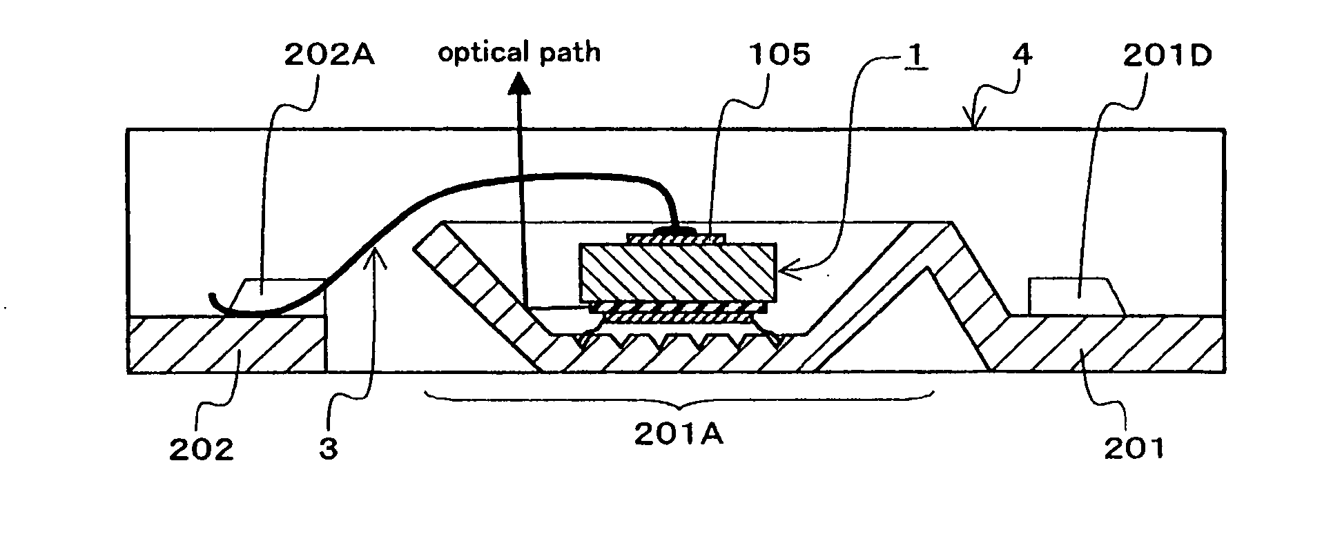
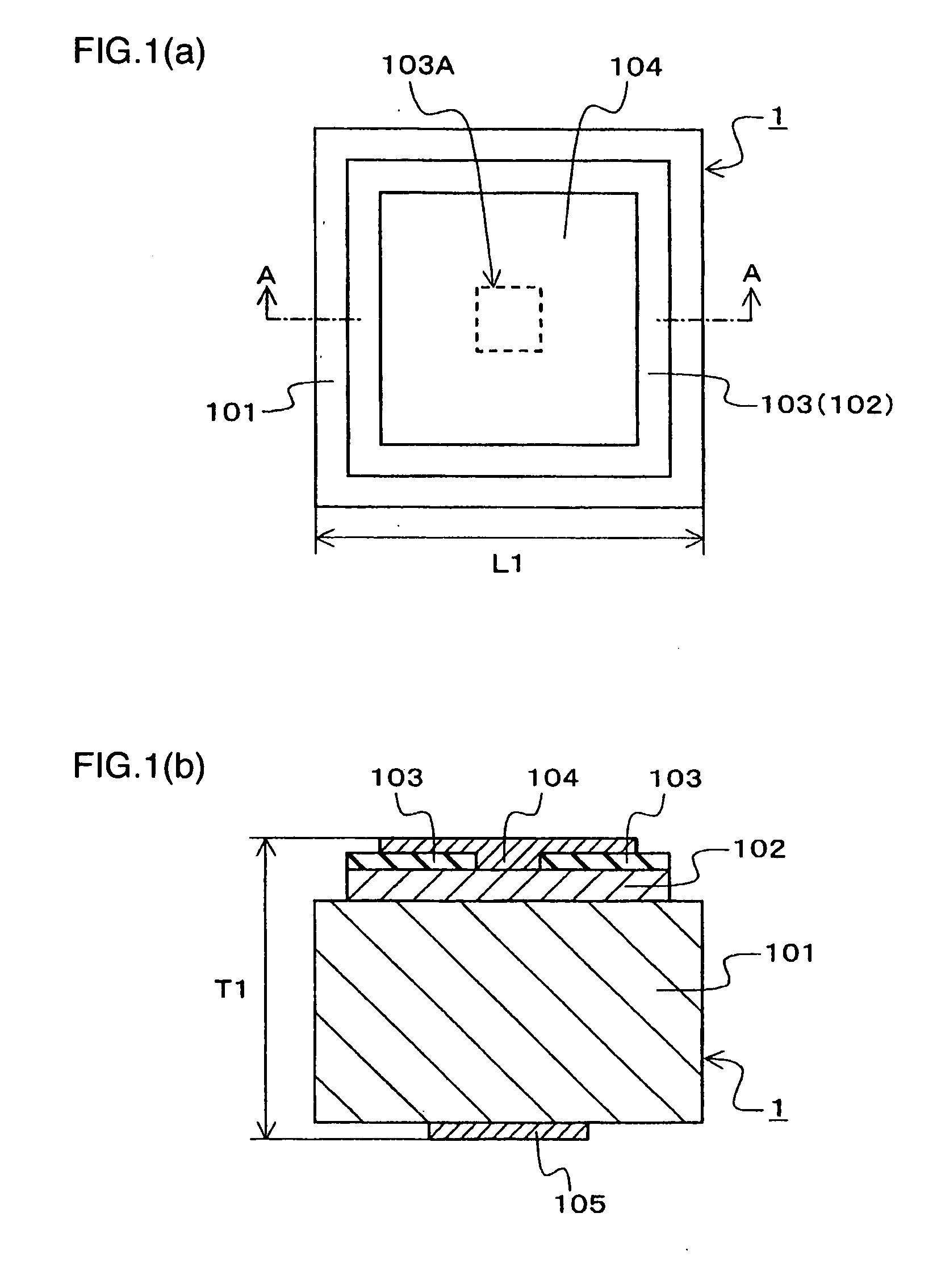
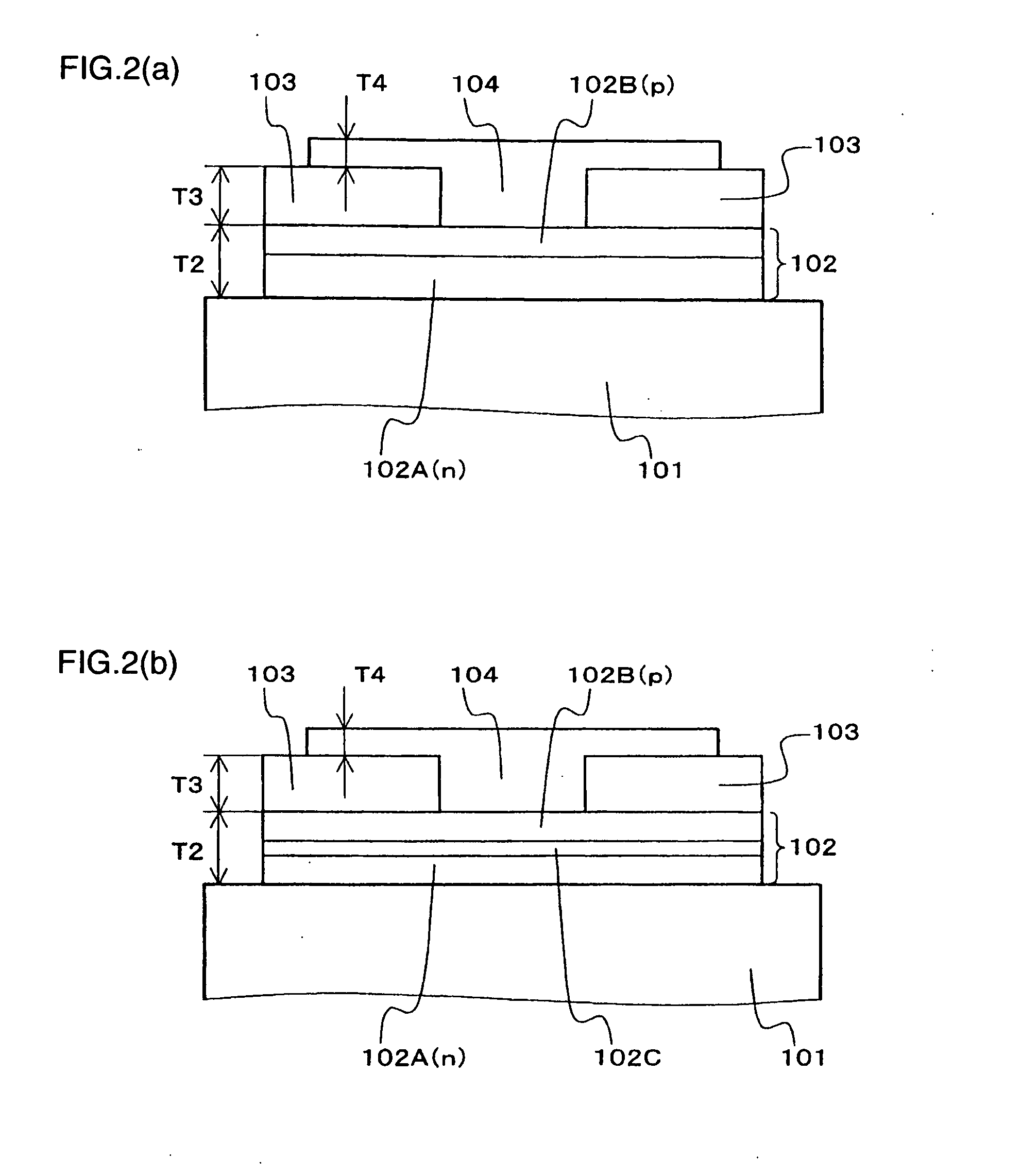
[0055] FIGS. 3(a), 3(b), 3(c), 4(a), 4(b), and 4(c) are schematic views showing general constitutions of a light-emitting device according to the embodiment of the present invention; FIG. 3(a) is a plan view of a light-emitting device as viewed in a light-emitting direction; FIG. 3(b) is a cross-sectional view along B-B line in FIG. 3(a); FIG. 3(c) is a magnified cross-sectional view of the joining part of the first electrode of a light-emitting element and the first lead; FIG. 4(a) is a plan view showing a constitution of an element mounting part of the first lead; FIG. 4(b) is a cross-sectional view along C-C line in FIG. 4(a); and FIG. 4(c) is a sectional view along D-D line in FIG. 3(a).

[0056] In each of FIGS. 3(a), 3(b), 3(c), 4(a), 4(b), and 4(c), 201 is the first lead, 201A is an element mounting part, 201B and 201C are grooves, 201D is a protruding portion as preventive measures for dropping, 202 is the second lead, 202A is a protruding portion as preventive measures for dr...


PUM


Abstract

A method for producing a light-emitting device comprising: a step of electrically connecting a first electrode provided on one main surface of a semiconductor substrate (element substrate) through a light-emitting layer, and a first lead of a lead frame, so as to oppose each other; a step of electrically connecting a second electrode provided on the rear surface of a surface provided with the light-emitting layer of said element substrate, and a second lead of the above-described lead frame; a step of encapsulating a connecting part of said first electrode and said first lead, and said second electrode, and an electrode part of the second lead, with a transparent resin; and a step of producing a discrete edge by cutting said first lead and the second lead from said lead frame; wherein a film of joining material (joining material film) made of an alloy or a single metal, is formed on the first electrode of said light-emitting element, and a pattern to reduce spreading of said joining material is formed on an element mounting part of said first lead, in advance of the step of electrically connecting the first electrode of said light-emitting element and said first lead, to reduce amount of the joining material flowing outside of a joining area wherein the first electrode is placed.

Description

TECHNICAL FIELD [0001] The present invention relates to a method for producing a light-emitting device and a light-emitting device, and in particular, relates to effective technology to be applied to a light-emitting device in which a light-emitting layer side provided on a semiconductor substrate (element substrate) is mounted (joined) as opposing to a lead frame. BACKGROUND ART [0002] There has conventionally been a light-emitting device using a light-emitting element provided with a light-emitting layer on one main surface of a semiconductor substrate, such as LED (Light Emitting Diode) and LD (Laser Diode). When the light-emitting device is produced, a lead frame having an opening part, with the first lead electrically connected with one electrode of the light-emitting element, and the second lead electrically connected with the other electrode, both projecting to the opening part, is used. In this case, for example, an element mounting part to mount the light-emitting element i...

Claims


Application Information

Patent Timeline
IPC IPC(8): H01L33/00H01L33/48H01L33/38H01L33/54H01L33/56H01L33/62H01S5/02H01S5/0232H01S5/042
CPCH01L23/49503H01L2224/29339H01L24/33H01L24/48H01L24/97H01L33/486H01L33/54H01L33/60H01L33/62H01L2224/29111H01L2224/32014H01L2224/32057H01L2224/32245H01L2224/48091H01L2224/48247H01L2224/48465H01L2224/73265H01L2224/83191H01L2224/83385H01L2224/97H01L2924/01013H01L2924/01029H01L2924/01033H01L2924/01047H01L2924/0105H01L2924/01078H01L2924/01079H01L2924/01082H01L2924/10329H01L2924/10336H01L2924/1815H01L2924/3011H01S5/0071H01S5/02228H01S5/0224H01S5/02272H01S5/02292H01S5/0425H01L2924/0132H01L2924/01005H01L2924/01006H01L2924/01023H01L2924/01074H01L2924/01322H01L2224/92247H01L2924/15747H01L2224/29139H01L2924/12041H01L2224/2929H01L24/32H01L2924/00014H01L2224/85H01L2224/83H01L2924/00H01L2924/01014H01L2924/01031H01L2924/00012H01L2924/3512H01L2924/0665H01L2224/32257H01L2224/26175H01L2924/351H01L2924/181H01L24/73H01S5/02234H01S5/0234H01S5/02255H01S5/0237H01S5/02345H01S5/0232H01L2224/45099H01L2224/45015H01L2924/207
Inventor OHNO, EJIJITAKAHASHI, SYOICHIKAWAMURA, MIKIYOSHIYAMAMURA, MINORUTAMAKI, TADASHIOBA, HAYATOKAGIWADA, MASATAKATAKAYAMA, HIROYUKITERAMURA, KEIOHTAKA, ATSUSHIMORIKAWA, TOSHIAKI
Owner STANLEY ELECTRIC CO LTD
Why Eureka
Try Eureka