Structure comprising 3-dimensional integrated circuit architecture, circuit structure, and instructions for fabrication thereof

a technology of integrated circuits and circuit structures, applied in the direction of instruments, solid-state devices, semiconductor devices, etc., can solve problems such as competing processing requirements

Active Publication Date: 2007-12-06
IBM CORP
View PDF6 Cites 214 Cited by
  • Summary
  • Abstract
  • Description
  • Claims
  • Application Information

AI Technical Summary

Benefits of technology

[0010] The design structure includes: (1) a first memory array disposed, located or formed upon a first substrate layer and having a first performance and power specification; (2) a second memory array different from the first memory array and disposed, located or formed upon a second substrate layer different from the first substrate layer and having a second power and performance specification different from the first power and performance specification; and (3) a plurality of logic circuit elements disposed, located or formed upon a third substrate layer coupled to the first memory array and the second memory array. The foregoing dispositions of the first memory array, second memory array and plurality of logic elements upon separate substrate layers allows for individual optimization of the devices or circuits that comprise the first memory array, the second memory array and the plurality of logic circuit elements.

Problems solved by technology

The optimization of performance characteristics of various semiconductor circuits and semiconductor devices often leads to competing processing requirements.

Method used


Image

  • Structure comprising 3-dimensional integrated circuit architecture, circuit structure, and instructions for fabrication thereof
  • Structure comprising 3-dimensional integrated circuit architecture, circuit structure, and instructions for fabrication thereof
  • Structure comprising 3-dimensional integrated circuit architecture, circuit structure, and instructions for fabrication thereof

Examples


Embodiment Construction

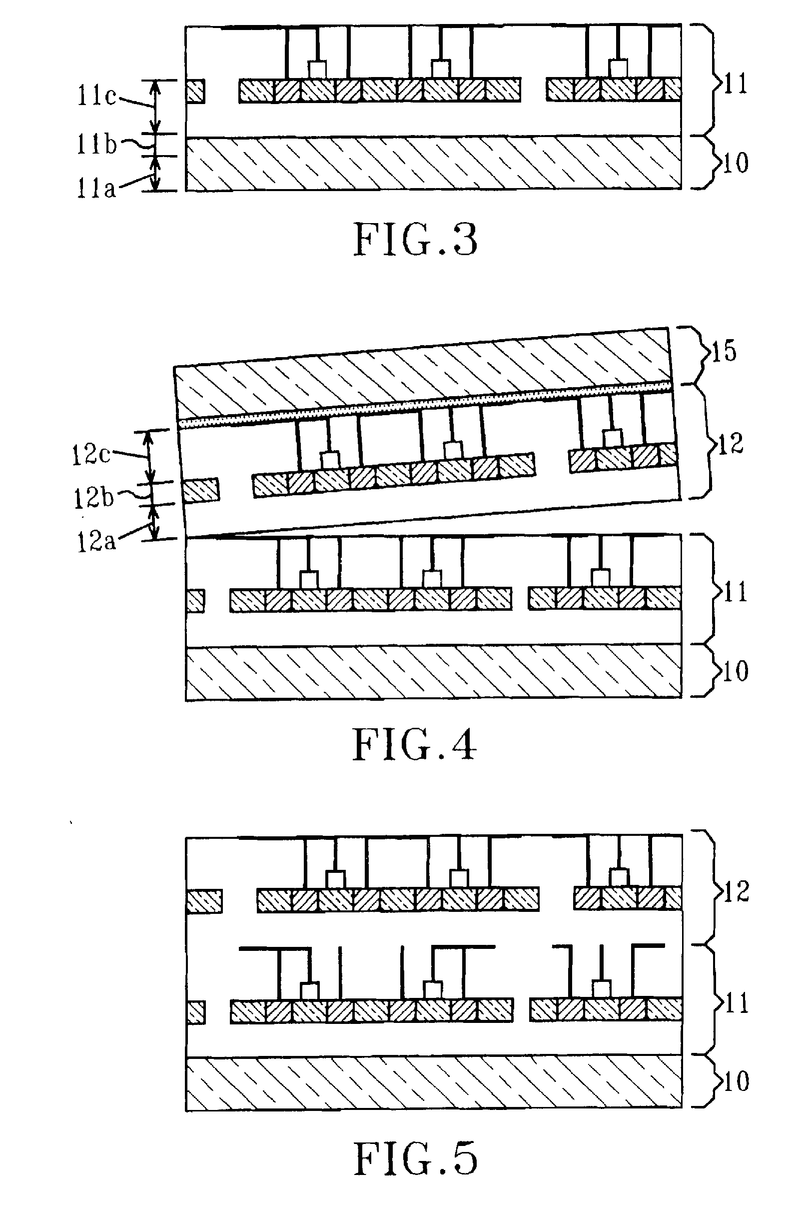
[0019] The embodiments and the invention, which include a design structure instantiated in a computer readable medium further comprising an integrated circuit architecture, a related integrated circuit structure, and instructions for a method of fabrication thereof, are described in greater detail below within the context of the drawings described above. The drawings are intended for illustrative purposes, and as such they are not necessarily drawn to scale.

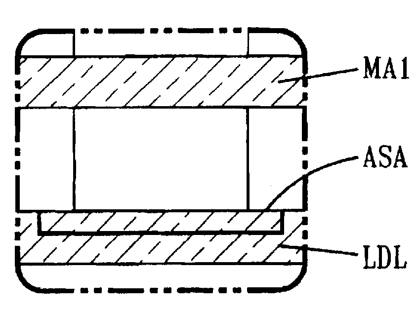
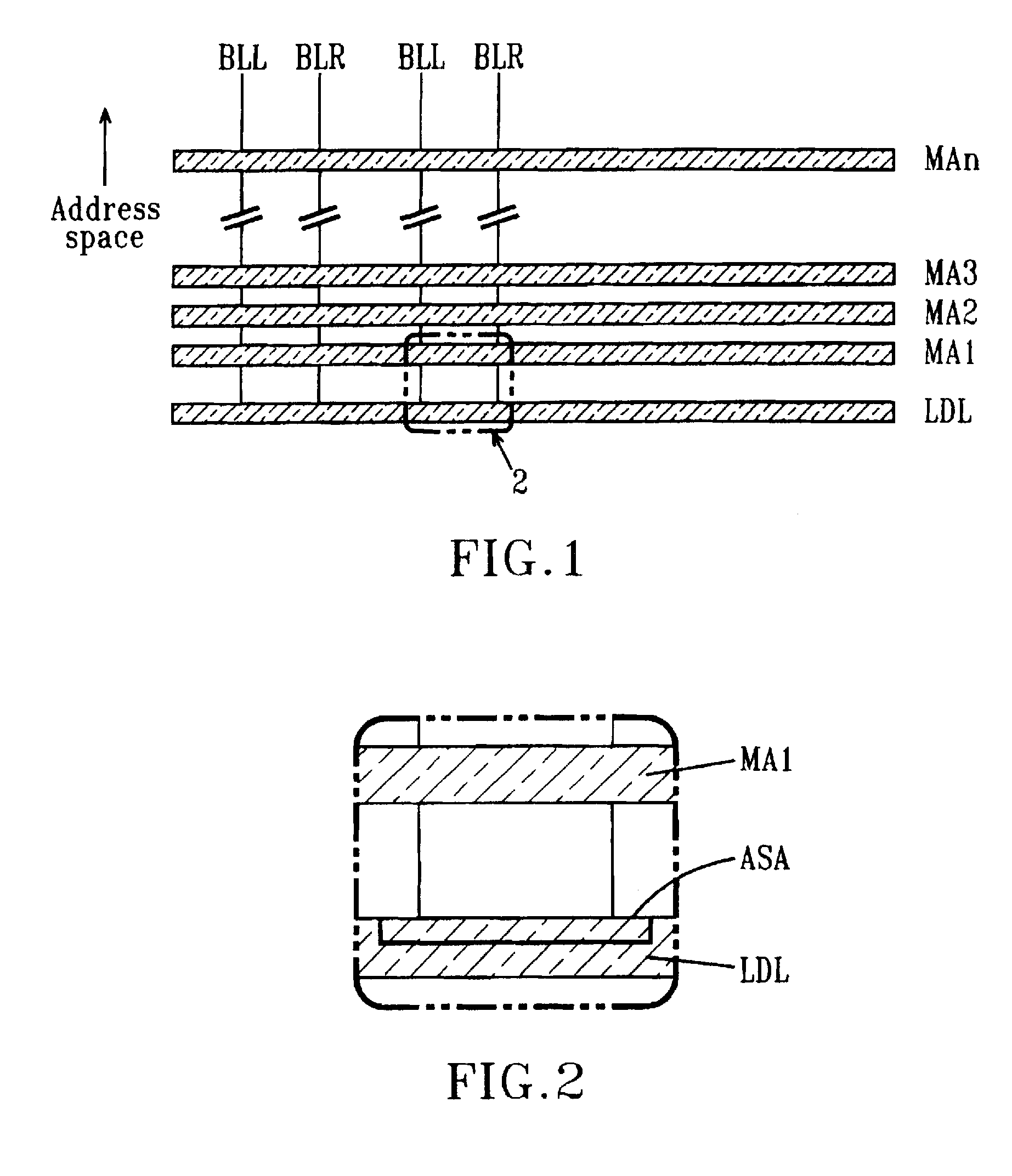
[0020]FIG. 1 shows a schematic diagram of an integrated circuit architecture that comprises an aspect and embodiment of the invention.

[0021] The integrated circuit architecture first comprises a logic device layer LDL (i.e., at least one logic device layer). The logic device layer LDL is intended to comprise a substrate or a substrate layer that includes logic devices located, disposed and formed therein. Logic devices are typically transistors, more typically field effect transistors. However, the invention is not limited to a...


PUM


Abstract

A design structure comprising an integrated circuit architecture, circuit structure, and/or instructions for fabrication thereof. The circuit structure includes at least one logic device layer and at least two additional separate memory array layers. Each of the logic device layer and the at least two memory array layers is independently optimized for a particular type of logic device or memory device disposed therein. Preferably also disposed within the logic device layer are array sense amplifiers, memory array output drivers and like higher performance circuitry otherwise generally disposed within memory array layer substrates. All layers may be independently powered to provide additional performance enhancement.

Description

CROSS-REFERENCE TO RELATED APPLICATIONS [0001] This application is a continuation in part of U.S. patent application Ser. No. 11 / 278,189, filed Mar. 31, 2006, which is assigned to the present assignee.BACKGROUND [0002] 1. Field of the Invention [0003] The invention relates generally to machine readable media having a design structure that embodies integrated circuit architectures (i.e., designs), related integrated circuit structures and instructions for fabrication thereof. More particularly, the invention relates to a data structure comprising enhanced performance integrated circuit architectures, related integrated circuit structures and instructions for fabrication thereof. [0004] 2. Description of the Related Art [0005] Modern semiconductor circuits often integrate circuit types or components, such as transistors, resistors and capacitors, for which different types of performance characteristics are desirably optimized. For example, field effect transistors that are used within...

Claims


Application Information

Patent Timeline
Patent Type & Authority Applications(United States)
IPC IPC(8): G06F17/50
CPCH01L21/6835H01L21/8221H01L27/0688H01L27/105H01L2221/68359H01L27/1052H01L2924/14H01L2924/1433H01L2924/19041H01L2924/19043H01L2924/30105H01L2225/06541G06F30/00H10B99/00
Inventor BERNSTEIN, KERRYCOTEUS, PAUL WILLIAMEMMA, PHILIP GEORGE
Owner IBM CORP
Why Eureka
Try Eureka