Semiconductor Device with Improved Contacts

a technology of a semiconductor and a contact, applied in the field of metallurgical systems, can solve the problems of metallurgical interface challenges, metallurgical requirements affecting bga packages, and metallurgical challenges, and achieve the effect of low cost and robustness

Active Publication Date: 2007-12-13
TEXAS INSTR INC
View PDF16 Cites 6 Cited by
  • Summary
  • Abstract
  • Description
  • Claims
  • Application Information

AI Technical Summary

Benefits of technology

[0005] Applicant recognizes a need for a flexible, yet low-cost and robust methodology to fabricate devices with solder joints, especially semiconductor packages, so that the joints bestow application-specific mechanical and thermal reliability to the devices and the devices will pass product-specific tests.
[0007] The first alloys, dominated by copper / tin alloys, help to improve the drop test performance to the best level achieved by solder joints with copper pads. The second alloys, dominated by nickel-containing alloys, help to improve the life test performance by slowing the aging conditions.

Problems solved by technology

Recently, however, there are challenging requirements affecting BGA packages.
To name just a few: More and more, the solder elements are required to be free of lead (for environmental reasons); this requirement causes metallurgical challenges.
The contact pads have copper as its base metal; this choice creates metallurgical interface challenges for the solder elements.
The ever decreasing feature size of the package components creates new hurdles to pass the accelerated stress tests at acceptable survival rates; for instance, accelerated life tests at elevated temperatures and in moist environment become more challenging.

Method used


Image

  • Semiconductor Device with Improved Contacts
  • Semiconductor Device with Improved Contacts
  • Semiconductor Device with Improved Contacts

Examples


Embodiment Construction

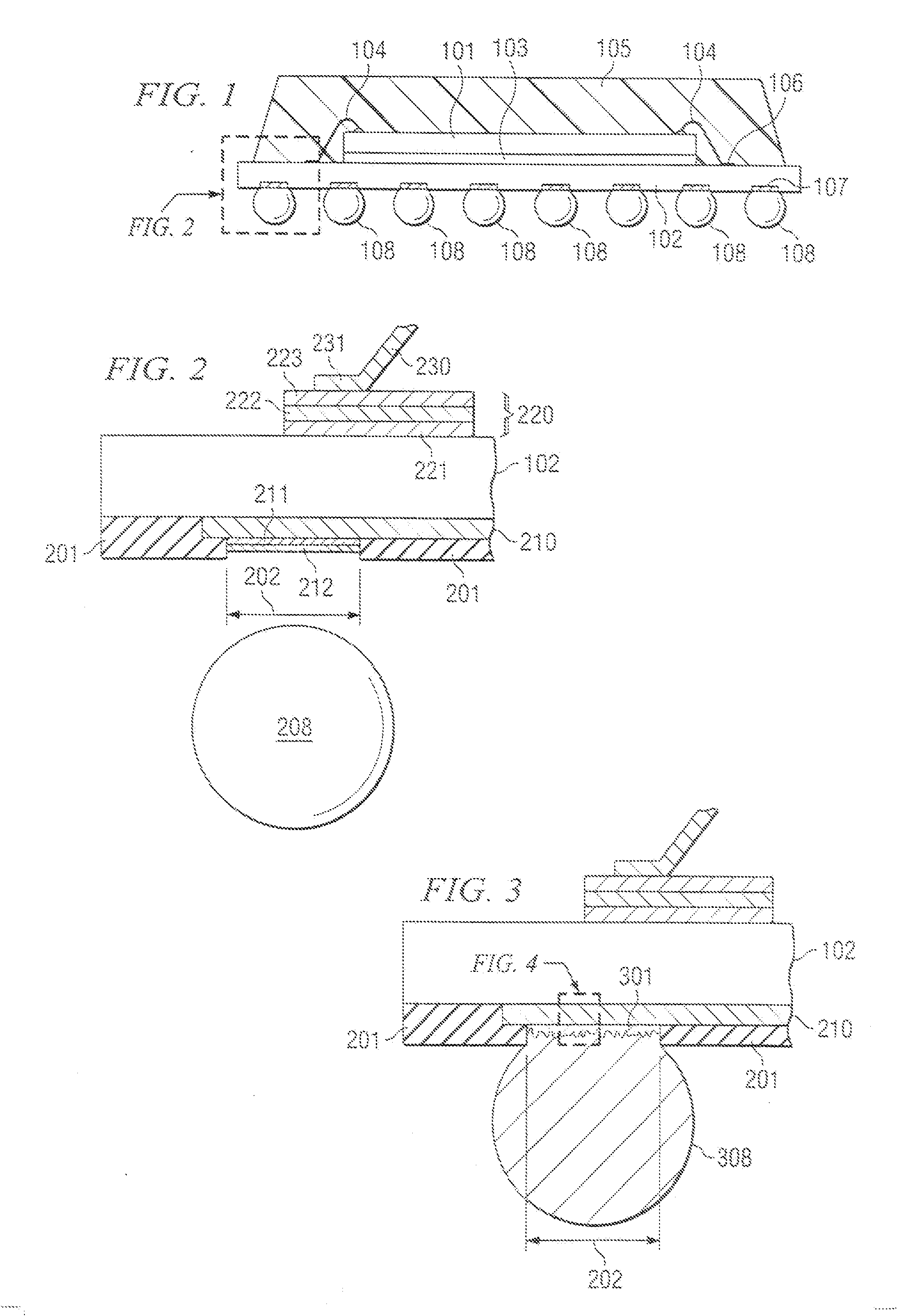
[0016]FIG. 1 illustrates schematically a representative of the large family of ball grid array (BGA) semiconductor devices. Semiconductor chip 101 is assembled on substrate 102 by using chip attach material 103 for mechanical attachment and bonding wires 104 for electrical connections. The assembly is encapsulated, typically in molding compound 105.

[0017] Substrate 102 has one or more patterned metal layers for internal interconnection (not shown in FIG. 1), especially to create connecting lines between the wire stitch bond sites 106 and the contact pads 107 for external connections. The metal layers are separated by insulating layers. Solder elements 108 are attached to the contact pads 107. The reliability of this solder attachment under various test and use conditions deserves special consideration.

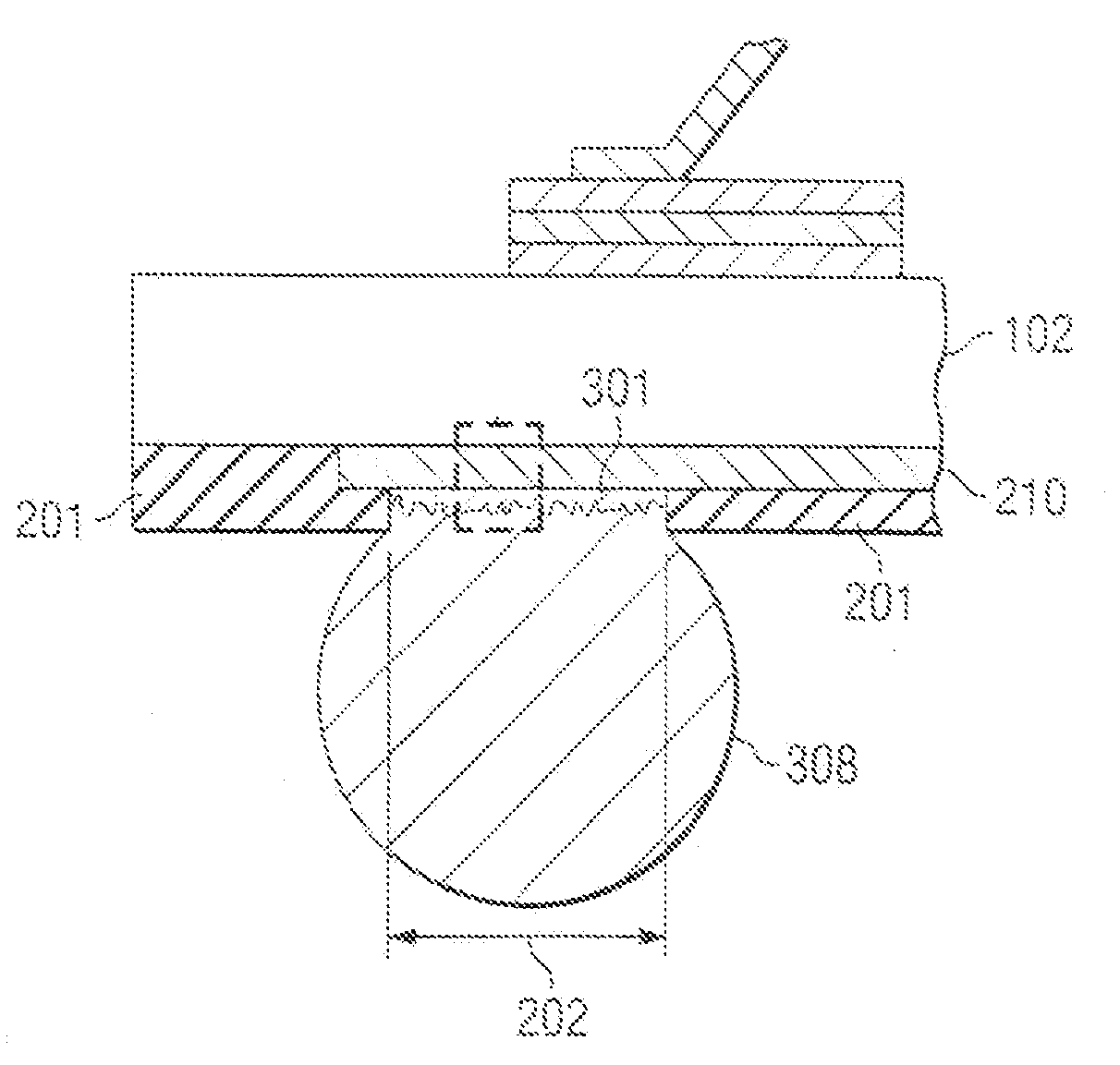
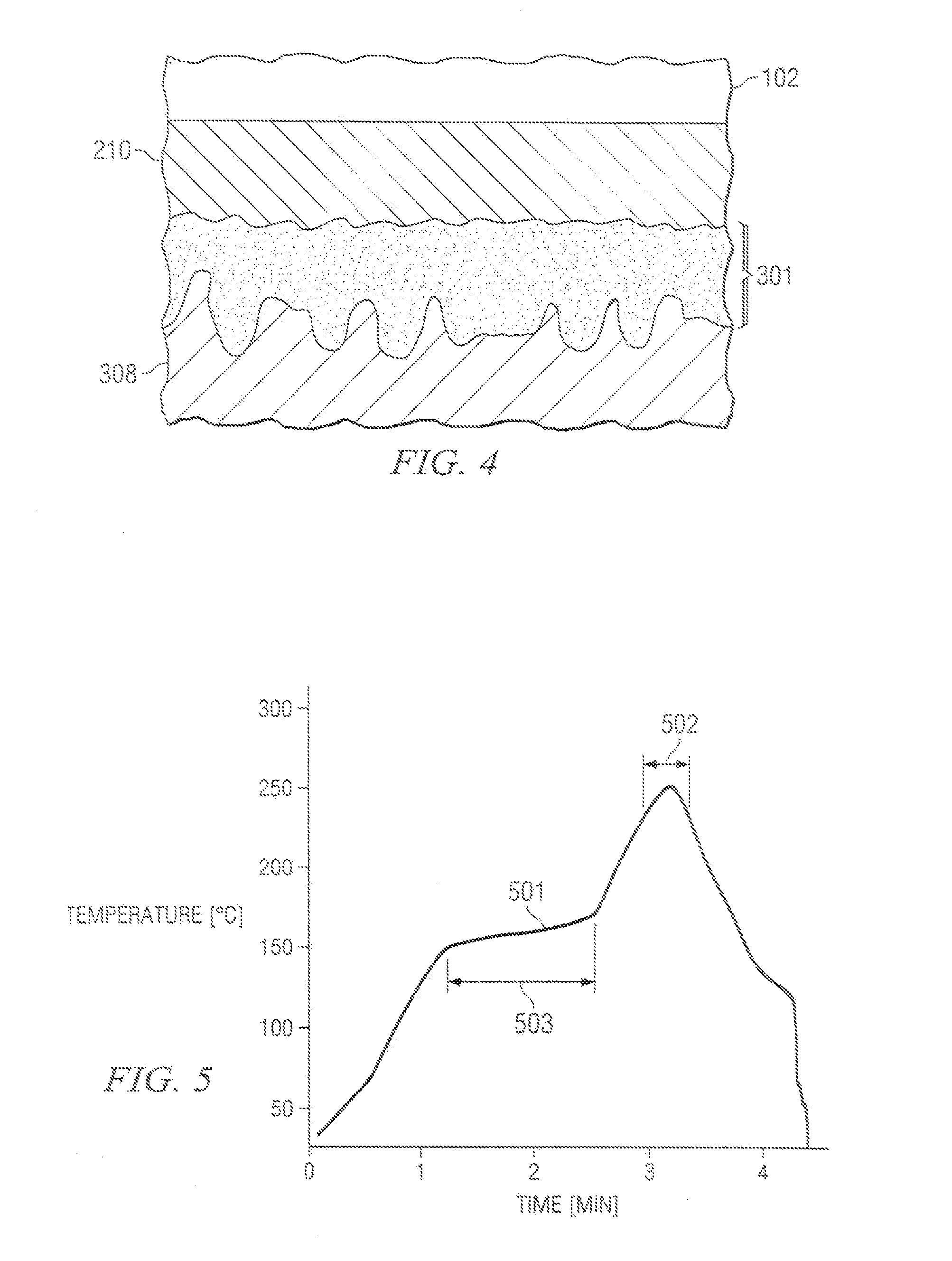
[0018] Portion “A” of the device is shown in more detail in FIGS. 2 and 3. FIG. 2 illustrates a device contact pad before the reflow of solder element 208, and FIG. 3 after the reflo...


PUM

PropertyMeasurementUnit
temperatureaaaaaaaaaa

Abstract

A device with a solder joint made of a copper contact pad (210) of certain area (202) and an alloy layer (301) metallurgically attached to the copper pad across the pad area. The alloy layer contains copper / tin alloys, which include Cu6Sn5 intermetallic compound, and nickel / copper / tin alloys, which include (Ni,Cu)6Sn5 intermetallic compound. A solder element (308) including tin is metallurgically attached to the alloy layer across the pad area. No fraction of the original thin nickel layer is left after the reflow process. Copper / tin alloys help to improve the drop test performance, nickel / copper / tin alloys help to improve the life test performance.

Description

[0001] This application is a continuation of application Ser. No. 11 / 201,717 filed Aug. 11, 2005, the contents of which are herein incorporated by reference in its entirety.FIELD OF THE INVENTION [0002] The present invention is related in general to the field of metallurgical systems with application to electronic systems and semiconductor devices, and more specifically to the structure of semiconductor devices with copper-metallized contact pads and their reliability under accelerated stress tests. DESCRIPTION OF THE RELATED ART [0003] Among the semiconductor device packages for surface mount assembly, ball grid array (BGA) packages enjoy an ever increasing popularity. They can be used in many customer products and lend themselves to the ongoing trend of miniaturization. The solder elements, distributed over the whole package area, offer high numbers of input / output terminals. In addition, the solder elements offer the opportunity of board attach technology at very low failure rate...

Claims


Application Information

Patent Timeline
Patent Type & Authority Applications(United States)
IPC IPC(8): H01L23/48
CPCH01L23/498H01L2924/0002H01L24/45H01L24/48H01L24/85H01L2224/32225H01L2224/45144H01L2224/48227H01L2224/48465H01L2224/48599H01L2224/73265H01L2224/85444H01L2924/01005H01L2924/01015H01L2924/01028H01L2924/01029H01L2924/0103H01L2924/01033H01L2924/01046H01L2924/01047H01L2924/01049H01L2924/0105H01L2924/01051H01L2924/01078H01L2924/01079H01L2924/01082H01L2924/01083H01L2924/01327H01L2924/014H01L2924/14H01L2924/15311H01L2924/3025H05K3/244H05K3/3463H01L23/49816H01L2224/0401H01L2224/48799H01L2224/05548H01L2224/05567H01L2224/13022H01L2924/01006H01L2224/45147H01L2924/00014H01L2924/00H01L2924/00012H01L2224/05552H01L2924/181H01L2224/48844H01L2224/48644H01L24/73H01L2924/00011H01L23/48H01L23/52H01L29/40
Inventor ANO, KAZUAKI
Owner TEXAS INSTR INC
Why Eureka
Try Eureka