Method and Apparatus for Secure Configuration of a Field Programmable Gate Array

a gate array and secure configuration technology, applied in the field of integrated circuits, can solve the problems of lack of user design security, difficult to “clone” a product containing a mask, and the sram programmed fpgas. achieve the effect of compromising the ease of manufactur

Inactive Publication Date: 2007-12-13
ALGOTRONIX
View PDF62 Cites 65 Cited by
  • Summary
  • Abstract
  • Description
  • Claims
  • Application Information

AI Technical Summary

Benefits of technology

[0034] A feature of this invention is to provide a cryptographic security protocol which prevents unauthorized third parties from reverse engineering FPGA bitstreams or benefiting economically from manufacturing clone products containing pirate copies of FPGA bitstreams.
[0035] Another feature of this invention is to provide this security without requiring on chip nonvolatile memory cells or individual customization steps for every chip in the manufacturing process.
[0036] Another feature of this invention is to prevent pirates from removing copyright messages from cloned designs and to allow FPGA users to trace the individual product unit from which a design has been cloned.
[0037] A further feature of this invention is to provide an FPGA implemented with a standard processing flow that can securely store cryptographic keys needed to support a protocol for securely downloading programming information over a communications network into an external memory.
[0038] This invention further provides security without compromising the ease of manufacture of the SRAM FPGAs, without complicating the Computer Aided Design tools for the SRAM FPGAs, and without removing the user's ability to reprogram the SRAM FPGAs many times.

Problems solved by technology

A shortcoming of FPGAs, especially SRAM programmed FPGAs, is a lack of security of the user's design because the configuration bitstreams may be monitored as they are being input into the FPGA.
It is very difficult to “clone” a product containing a mask programmed ASIC or one of the nonvolatile FPGAs.
Cloning an ASIC involves determining the patterning information on each mask layer which requires specialist equipment and a significant amount of time.
It is also difficult to copy configuration information loaded into the nonvolatile FPGA technologies after their “security fuses” have been blown—thus these devices are attractive to customers who have concerns about their design being pirated or reverse engineered.
This security problem of SRAM FPGAs has been well known in the industry for at least 10 years and to date no solution attractive enough to be incorporated in a commercial SRAM FPGA has been found.
Present day FPGAs have a relatively high power consumption even when the user logic is not operating: which limits the life span of the battery back up.
If power is lost for even a fraction of a second the system the FPGA control memory will no longer be valid and the system will cease to function.
This raises concerns about the reliability of a system which uses this technique.
Thus, this prior art approach to protecting FPGA bitstreams is only applicable to a small fraction of FPGA applications.

Method used


Image

  • Method and Apparatus for Secure Configuration of a Field Programmable Gate Array
  • Method and Apparatus for Secure Configuration of a Field Programmable Gate Array
  • Method and Apparatus for Secure Configuration of a Field Programmable Gate Array

Examples


Embodiment Construction

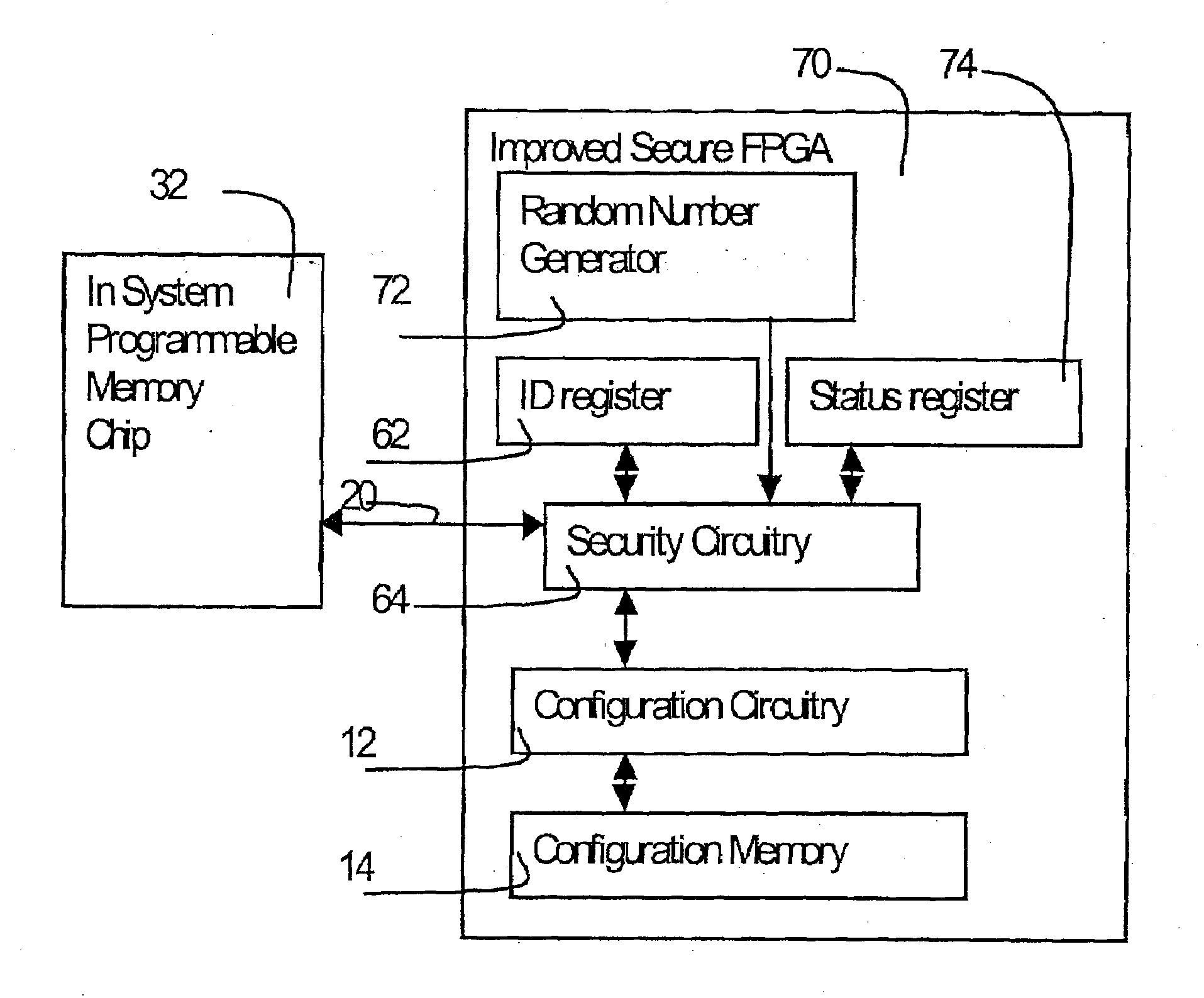
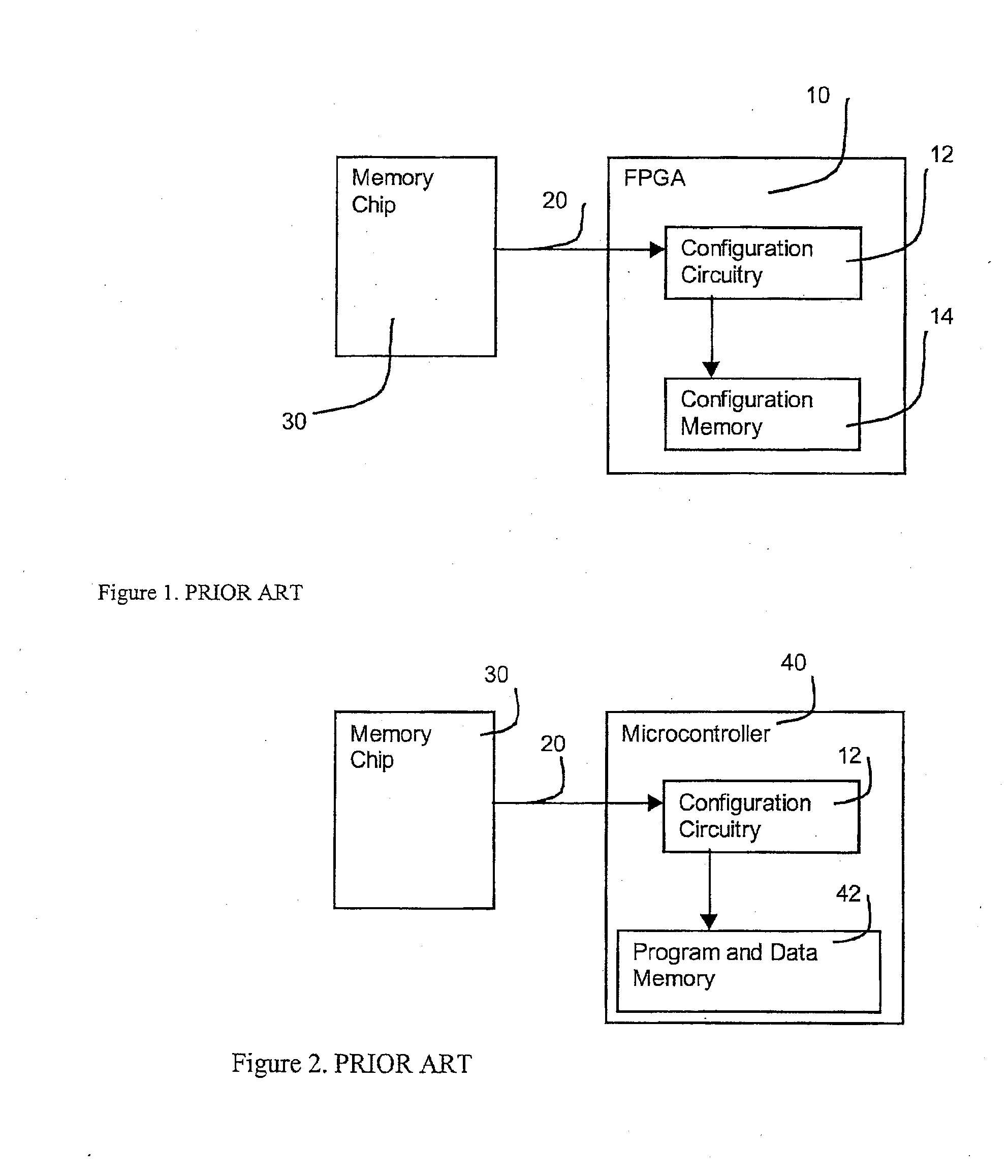
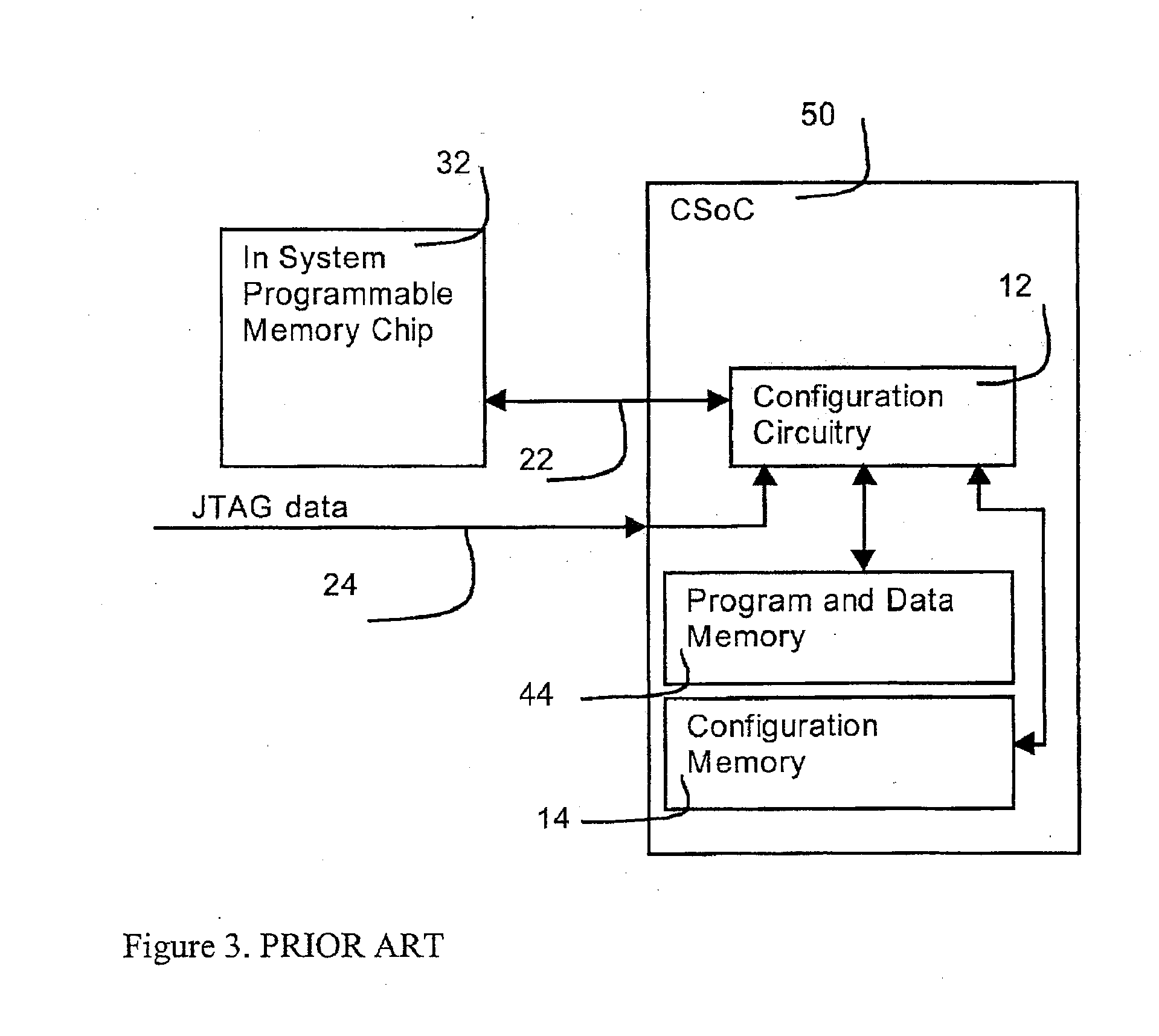
[0049]FIG. 1 shows a prior art SRAM programmed FPGA 10 connected to a memory chip 30 via a set of signal traces 20 on a printed circuit board. Configuration circuitry 12 on the FPGA loads programming data from memory 30 into on chip configuration memory 14. Resources on the FPGA not related to programming (such as the logic gates and routing wires which implement the user design) are not shown in this or subsequent illustrations for reasons of clarity but are well understood and are described in manufacturer's literature such as Xilinx Inc. “Virtex 2.5 V Field Programmable Gate Arrays,” Advanced Product Specification, 1998 and the Oldfield and Dorf textbook mentioned above. Set of signals 20 will normally include a data signal to transfer configuration information, a clock signal to synchronize the transfer and several control signals to specify a particular mode of transfer (for example when a sequence of FPGAs can be daisy chained to a single source of programming data). The exact...


PUM


Abstract

A field programmable gate array has security configuration features to prevent monitoring of the configuration data for the field programmable gate array. The configuration data is encrypted by a security circuit of the field programmable gate array using a security key. This encrypted configuration data is stored in an external nonvolatile memory. To configure the field programmable gate array, the encrypted configuration data is decrypted by the security circuit of the field programmable gate array using the security key stored in the artwork of the field programmable gate array. The secret key comprises a number of bits of key information that are embedded within the photomasks used in manufacture the FPGA chip.

Description

[0001] This application is a continuation of U.S. patent application Ser. No. 09 / 780,618, filed on Feb. 8, 2001, now issued as U.S. Pat. No. 7,240,218, which claims priority to UK patent application GB 0002829.0, filed Feb. 9, 2000 and U.S. provisional patent application 60 / 181,118, filed Feb. 8, 2000, and which is a continuation-in-part of U.S. patent application Ser. No. 09 / 747,759, filed on Dec. 21, 2000, now issued as U.S. Pat. No. 7,203,842, which claims priority to UK patent application GB9930145.9, filed Dec. 22, 1999 and U.S. provisional patent application 60 / 181,118, filed Feb. 8, 2000, all of which are hereby incorporated by reference herein, along with all references recited in this application.BACKGROUND OF THE INVENTION [0002] This invention relates to integrated circuits such as field programmable gate arrays (FPGAs) which contain an on-chip volatile program memory which must be loaded from an off-chip nonvolatile memory when power is applied before normal operation of...

Claims


Application Information

Patent Timeline
Patent Type & Authority Applications(United States)
IPC IPC(8): H04L9/32
CPCG06F21/76
Inventor KEAN, THOMAS A.
Owner ALGOTRONIX
Why Eureka
Try Eureka