
Timing controller for controlling pixel level multiplexing display panel

a display panel and timing controller technology, applied in the direction of instruments, static indicating devices, etc., can solve the problem that the conventional timing controller cannot be used in this panel, and achieve the effect of saving costs

Active Publication Date: 2007-12-20
AU OPTRONICS CORP
View PDF3 Cites 5 Cited by
  • Summary
  • Abstract
  • Description
  • Claims
  • Application Information

AI Technical Summary

Benefits of technology

[0009]An objective of the present invention is to provide a timing controller for driving a pixel level multiplexing display panel, and particularly, the timing controller drives the pixel level multiplexing display panel without changing architectures of conventional scan and data driving circuits, thereby saving the cost.
[0015]In the present invention, as a new pixel level multiplexing display panel is employed in the present invention, and a timing controller is used to control the pixel level multiplexing display panel, the timing controller drives the pixel level multiplexing display panel without changing architectures of conventional scan and data driving circuits, therefore, the present invention not only can eliminate the restrictions on circuit design, enhance the selectivity on the circuit design, but also save the manufacturing cost.

Problems solved by technology

Therefore, the conventional timing controller cannot be used in this panel.

Method used


Image

  • Timing controller for controlling pixel level multiplexing display panel
  • Timing controller for controlling pixel level multiplexing display panel
  • Timing controller for controlling pixel level multiplexing display panel

Examples


Embodiment Construction

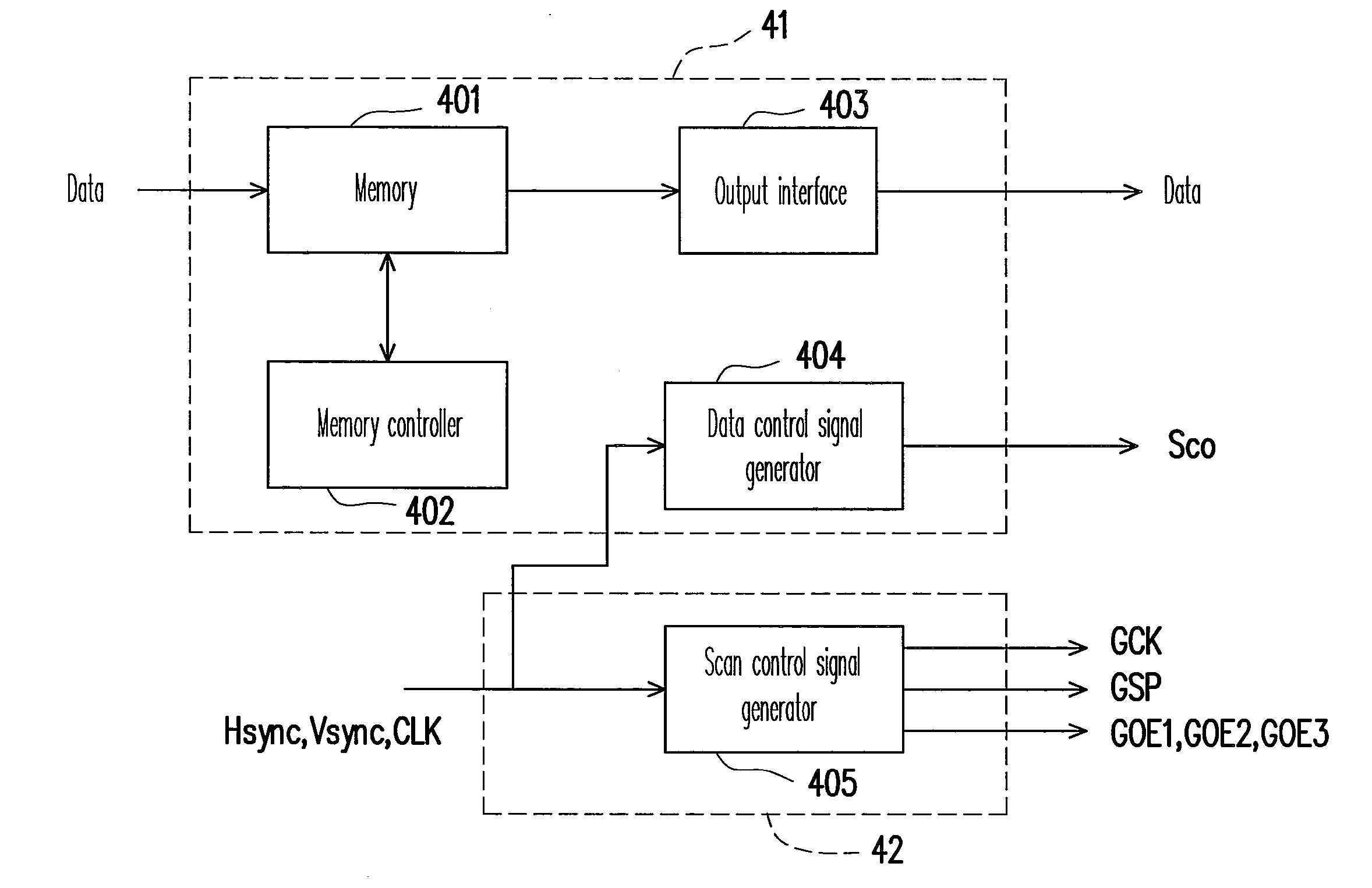
[0029]FIG. 4 shows a timing controller for controlling a pixel level multiplexing (PLM) display panel according to an embodiment of the present invention. The timing controller comprises a memory 401, a memory controller 402, an output interface 403, a data control signal generator 404 and a scan control signal generator 405. In order to facilitate the illustration, the pixel level multiplexing display panel in FIG. 3 is taken as an example of the panel controlled by the timing controller in this embodiment. However, those skilled in the art should know that the timing controller provided in the present invention may be used to control other similar types of pixel level multiplexing display panels, and thus, the present invention is not limited to this.

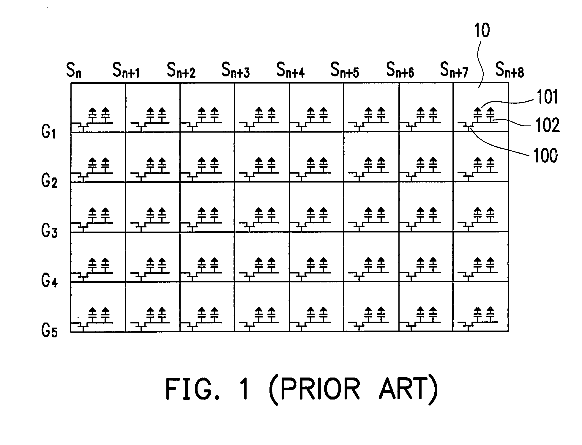
[0030]The pixel level multiplexing display panel of FIG. 3 mainly comprises 6 scan lines G1-G6 and 4 data lines Sn-Sn+6 disposed to be crossed with each other (in order to facilitate the illustration, a smaller display panel is used a...


PUM


Abstract

A timing controller including a memory and a memory controller is provided. The memory includes an odd-field block and an even-field block. The memory controller is coupled to the memory and controls the memory. When two of a first, a second and a third gate output enable signals output by the timing controller are active, the memory is controlled to output the data of the (I-1)th scan line stored in the odd-field block. When one of the first, the second and the third gate output enable signals output by the timing controller is active, and the other two signals are inactive, the memory is controlled to output the data of Jth scan line stored in the even-field block and write an odd-field field data of the (J+1)th scan line to the odd-field block and write an even-field field data of the (J+1)th scan line to the even-field block.

Description

CROSS-REFERENCE TO RELATED APPLICATION[0001]This application claims the priority benefit of Taiwan application serial no. 95121378, filed Jun. 15, 2006. All disclosure of the Taiwan application is incorporated herein by reference.BACKGROUND OF THE INVENTION[0002]1. Field of Invention[0003]The present invention relates to a driving circuit of a flat panel display, and more particularly, to a timing controller applicable for controlling a pixel level multiplexing display panel, and a timing controller that is provided without changing architectures of a conventional data driving circuit and a scan driving circuit.[0004]2. Description of Related Art[0005]Flat panel displays, such as a liquid crystal display (LCD), have been widely used in recent years. As the progress of the semiconductor technology, the liquid crystal display (LCD) panel has the advantages of low power consumption, being thin and light, high resolution, high color saturation, long life time, and so on, therefore, it h...

Claims


Application Information

Patent Timeline
IPC IPC(8): G09G3/36
CPCG09G3/3611G09G3/3659G09G2360/12G09G2310/08G09G2310/0251
Inventor SHEN, KUO-LIANGYI, CHIEN-YU
Owner AU OPTRONICS CORP
Learn More