Manufacturing process of embedded type flexible or rigid printed circuit board
a printed circuit board and flexible technology, applied in the manufacture of printed circuits, electrical appliances, cable/conductor devices, etc., can solve the problems of high cost, less attractive products, and difficult control and prediction of the price of raw materials by the purchasing department of the company, so as to enhance competitiveness and save costs
- Summary
- Abstract
- Description
- Claims
- Application Information
AI Technical Summary
Benefits of technology
Problems solved by technology
Method used
Image

Examples
first embodiment
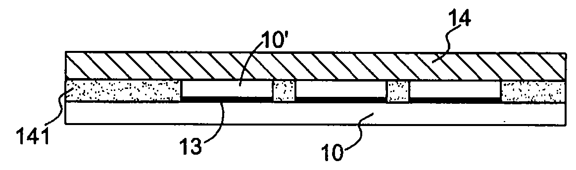
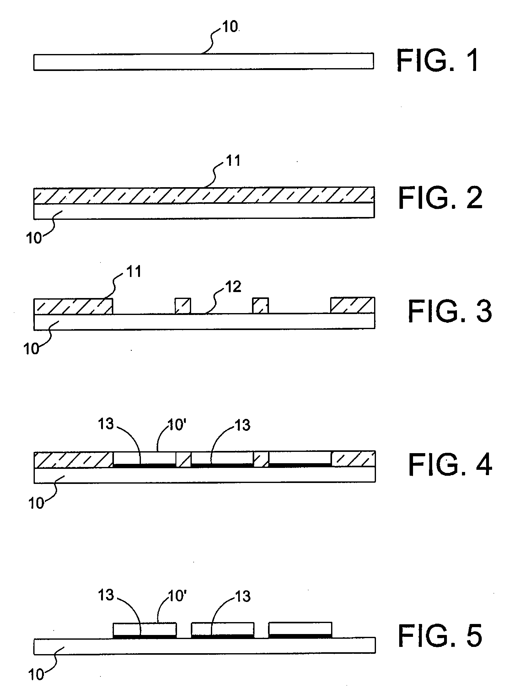
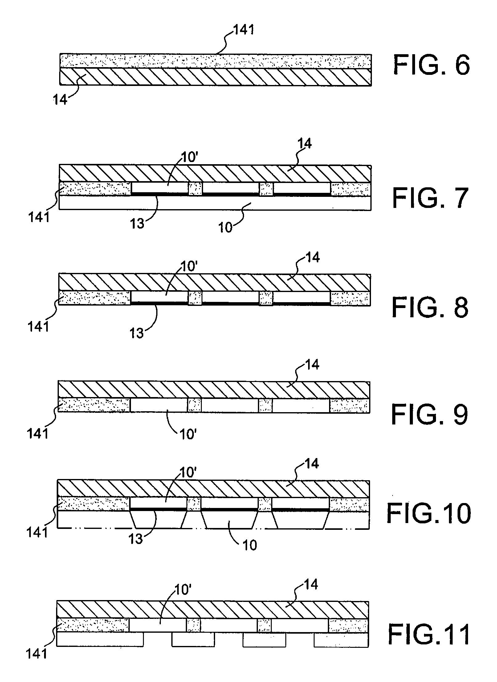
[0017]FIG. 1 to FIG. 11 illustrate the present invention. Referring to FIG. 1 to FIG. 9, a first step is to prepare a layer of copper foil 10 and the layer of the copper foil 10 is coated with a layer of dry film 11. A circuit pattern 12 is formed on the layer of the copper foil 10 after exposure and development of the dry film 11 by any conventional method. The layer of copper foil 10 is electroplated with an etching stop layer 13 of 3-10 um according to the circuit pattern 12. The etching stop layer 13 is electroplated with copper to form a first circuit 10′. Then the dry film 11 is removed from the layer of the copper foil 10. Next, the copper foil 10 is heated to become soft. A first organic layer 14 which includes an adhesive layer 141 is attached to the first circuit 10′ by coating, adhering or compressing. The first organic layer 14 is then solidified by heating or irradiating of ultraviolet light (UV). Alternatively, the first organic layer 14 can be directly coated on the f...
third embodiment
[0028] FIGS. 19 to 25 shows the present invention. The third embodiment distinguishes from the second embodiment in that the third embodiment starts from the structure of FIG. 9 rather than FIG. 7. FIG. 9 is formed after removing the layer of copper foil 10 and the etching stop layer 13 of FIG. 7. Specifically, as shown in FIG. 19, the third embodiment starts by forming a second organic layer 191 to cover the exposed first circuit 10′. Then, as shown in FIG. 20, at least one hole 201 through the second organic layer 191 is formed by any suitable method, such as laser drilling or lithography technology. Next, as shown in FIG. 21, a blanket conductive layer 211 is formed to cover the second organic layer 191 and fill up the hole 201 by electroplating. The filled hole 201 is referred to as a conductive via 211a. Subsequently, as shown in FIG. 22, the blanket conductive layer 211 is patterned to form a second circuit 221 by conventional lithography technology. Accordingly, the conductiv...
fourth embodiment
[0032]FIG. 26 shows the present invention. As shown in FIG. 26, a third laminate 260 is formed by pressing a stack having three insulating laminates 171 interlaced with two first laminates 230 and one conductive laminates 172 on the bottom of the stack. Next, a conductive via 263 interconnecting with each circuit level is built by drilling and electroplating. Then, an opening 261 is further formed to expose the first circuit 10′ by laser drilling. Subsequently, a blanket conductive layer 262 is formed to cover the top insulating laminates 171 and fill up the opening 121 by electroplating. The filled opening 261 is referred to as a conductive via 262a.
[0033] With the aforesaid steps, the manufacturing process of the embedded type flexible printed circuit board of the present invention does not need use of a conventional carrier, so as to greatly reduce costs. Moreover, the circuit board of the present invention can achieve the objectives of the portability and compactness with the s...
PUM
| Property | Measurement | Unit |
|---|---|---|
| thickness | aaaaa | aaaaa |
| conductive | aaaaa | aaaaa |
| flexible | aaaaa | aaaaa |
Abstract
Description
Claims
Application Information
 - R&D
- Intellectual Property
- Life Sciences
- Materials
- Tech Scout
- Unparalleled Data Quality
- Higher Quality Content
- 60% Fewer Hallucinations
Browse by: Latest US Patents, China's latest patents, Technical Efficacy Thesaurus, Application Domain, Technology Topic, Popular Technical Reports.
© 2025 PatSnap. All rights reserved.Legal|Privacy policy|Modern Slavery Act Transparency Statement|Sitemap|About US| Contact US: help@patsnap.com