Random number generating device

Active Publication Date: 2007-12-27
KK TOSHIBA
7 Cites 19 Cited by

AI-Extracted Technical Summary

Problems solved by technology

However, amplification of very low white noise requires a large amplifying circuit, making it difficult to obtain a small random number generating device.
Thus, thermal fluctuation causes random electron charging and discharging.
This randomly varies a current flowing through the channel, resulting in random noise.
However, the Si nano-crystal MOSFET produces only a low random noise ...

Benefits of technology

[0027]FIGS. 17A and 17B are diagrams showing an example of the configuration of a low pass filter...

Abstract

A random number generating device includes a semiconductor device including a source region, a drain region, a channel region provided between the source region and the drain region, and an insulating portion provided on the channel region, the insulating portion including a trap insulating film having traps based on dangling bonds and expressed by Six(SiO2)y(Si3N4)1-yMz (M is an element other than Si, O, and N, x≧0, 1≧y≧0, z≧0, the case where x=0 and y=1 and z=0 is excluded), conductivity of the channel region varying randomly depending on the amount of charge caught in the traps, and a random number generating unit connected to the semiconductor device and generating random numbers based on a random variation in the conductivity of the channel region.

Application Domain

Random number generatorsSemiconductor/solid-state device manufacturing +3

Technology Topic

EngineeringGenerating unit +5

Image

  • Random number generating device
  • Random number generating device
  • Random number generating device

Examples

  • Experimental program(7)

Example

FIRST EMBODIMENT
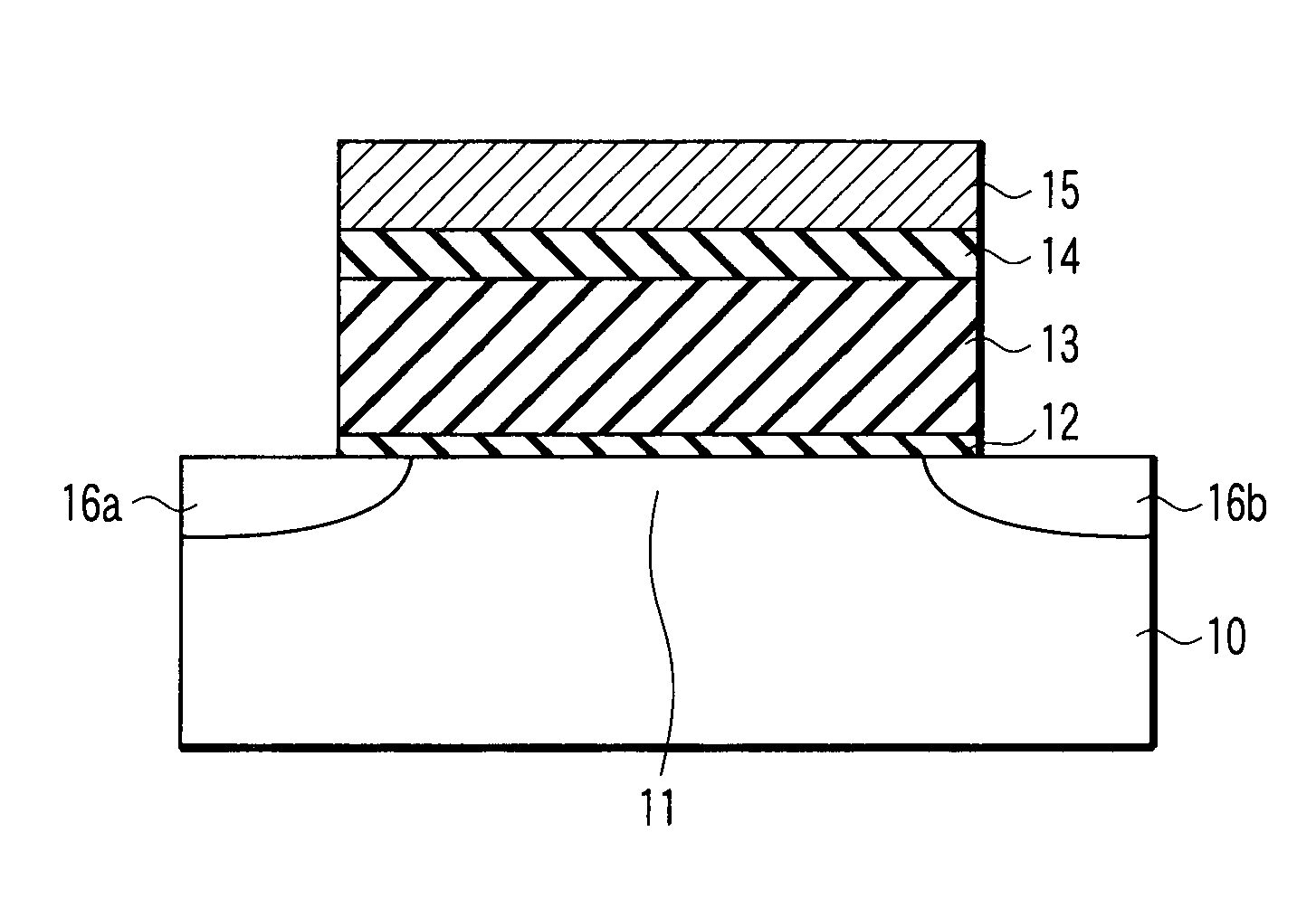
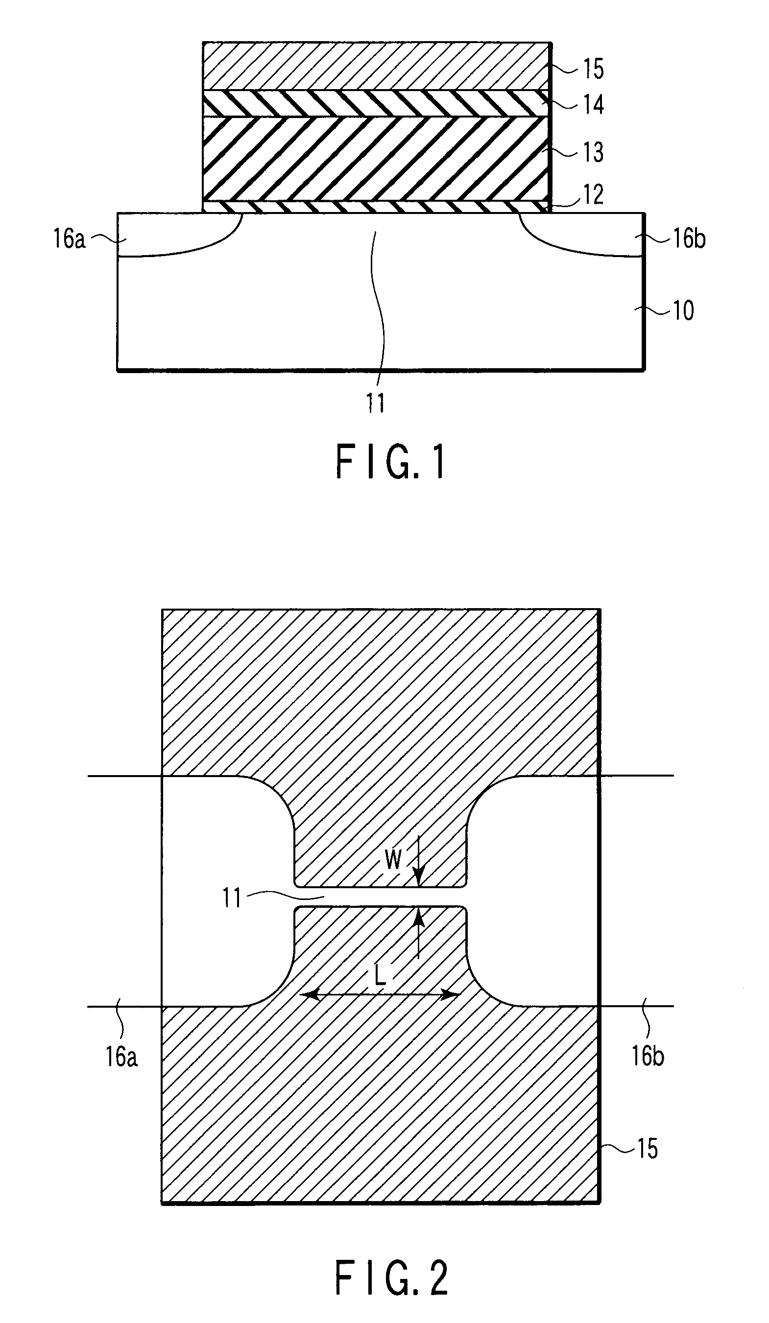
[0042] A noise generating device in accordance with the present embodiment uses a silicon oxide film as the tunnel insulating film 12 and an Si-rich silicon nitride film (SiUN:U=1) as the trap insulating film 13 (see FIG. 1).
[0043] First, a narrow channel pattern with a width W of 0.15 μm is formed on the silicon substrate 10 by trench isolation or the like. A tunnel insulating film 12 of thickness 0.7 nm is subsequently formed on the channel region 11 by thermal oxidation. An Si-rich silicon nitride film is further formed on the tunnel insulating film 12 as the trap insulating film 13. That is, an Si-rich silicon nitride film 13 (SiUN:U=1) with an Si/N ratio (ratio of the number of atoms) of 1 is formed by LPCVD with the ratio of Si source gas to N source gas adjusted. The Si-rich silicon nitride film 13 has a thickness of 20 nm.
[0044] Then, a control insulating film (control oxide film) 14 of thickness 6 nm is formed by LPCVD. An n+-type polysilicon film 15 of thickness 200 nm constituting a gate electrode is further formed by CVD. The n+-type polysilicon film 15 is subsequently patterned through a resist pattern as a mask to form a gate electrode 15. The gate electrode has a gate length L of 0.06 μm. Subsequently, phosphorus (P) or arsenic (As) is ion-implanted, and activation annealing is performed to form an n+-type diffusion layer constituting the source region 16a and the drain region 16b.
[0045] As described above, such a noise generating device as shown in FIG. 1 is formed. The noise generating device thus formed can generate random noise in which 1-MHz vibration component is at least 0.1%. Explanation will be given of the reason whey 1-MHz vibration component is at least 0.1% in the noise generating device in accordance with the present embodiment.
[0046]FIG. 6 shows the current fluctuation characteristic of the noise generating device in accordance with the present embodiment observed under a fixed bias. The gate length L is 0.06 μm, and the gate width W is 0.15 μm. The tunnel insulating film thickness T is 0.7 nm, and the Si/N ratio of the silicon nitride film 13 is 1. As shown in FIG. 6, the current fluctuation component is about 15% of the whole current.
[0047]FIG. 7 is a diagram showing the frequency characteristic of the current characteristic shown in FIG. 6. As seen in FIG. 7, a frequency in which current fluctuation component is 0.1% is about 2.8 MHz. A current fluctuation component at 1 MHz is about 0.16%. This satisfies the condition that the fluctuation component at 1 MHz is at least 0.1%.
[0048] Further, a noise generating device with different structural parameters was produced and its characteristics were examined. The structural parameters include the gate length L and channel width (gate width) W of the semiconductor narrow channel, the tunnel insulating film thickness T, and the ratio U of the silicon nitride film (SiUN, U>0.75).
[0049]FIG. 8 is a diagram showing the relationship between the gate length (channel length) L and a Fourier coefficient. W, T, and Si/N are 0.15 μm, 0.7 nm, and 1, respectively. The figure shows the relationship between the gate length L and the Fourier coefficient at 100 Hz. FIG. 8 indicates that the level of random noise is proportional to 1/L.
[0050]FIG. 9 is a diagram showing the relationship between the gate width (channel width) W and the Fourier coefficient. L, T, and Si/N are 0.06 μm, 0.7 nm, and 1, respectively. The figure shows the relationship between the gate width W and the Fourier coefficient at 250 Hz. FIG. 9 indicates that the level of random noise is proportional to W−2/5.
[0051]FIG. 10 is a diagram showing the relationship between the tunnel insulating film thickness T and the Fourier coefficient. L, W, and Si/N are 0.06 μm, 0.15 μm, and 1, respectively. The figure shows the relationship between the tunnel insulating film thickness T and the Fourier coefficient at 250 Hz. FIG. 10 indicates that the level of random noise is proportional to exp (−T/0.8664 [nm]).
[0052]FIG. 11 is a diagram showing the relationship between the ratio U of the silicon nitride film (SiUN, U>0.75) and the Fourier coefficient. L, W, and T are 0.06 μm, 0.15 μm, and 0.7 nm, respectively. The figure shows the relationship between the ratio U and the Fourier coefficient at 300 Hz.
[0053]FIG. 11 shows A×((U−0.75)/(1+U)+0.01174)1/2 as a theoretical model. Here, reference character A denotes a constant. This theoretical model is derived from the idea that the fluctuation is proportional to the ½ power of a superimposition number (trap density), on the basis of a statistical law. The term “trap density” as used herein refers to the number of dangling bonds per atom. With the silicon nitride film SiUN, stoichiometry is achieved at U=0.75. Thus, the number of dangling bonds per atom is (U−0.75)/(1+U). Accordingly, the relationship between the ratio of the number of atoms (the number of dangling bonds per atom) and the Fourier coefficient is expressed by the above theoretical model. Further, A×0.011741/2 at U=0.75 is a target value for noise intensity in the case where stoichiometry is achieved.
[0054] The above various experimental data are obtained by the present inventors on their own through experiments.
[0055] Conditions under which fluctuation component at 1 MHz is at least 0.1% in the Fourier coefficient for each parameter are shown below. FIG. 7 shows the dependence of the Fourier coefficient on the frequency observed when the gate length L, the gate width W, the tunnel insulating film thickness T, and the Si/N ratio are 0.06 μm, 0.15 μm, 0.7 nm, and 1, respectively. FIG. 7 indicates that a power law fitting equation for the Fourier coefficient is:
|Fourier Coe.|=0.0006f−0.4705
This equation enables the value of the Fourier coefficient for 0.1% fluctuation component to be estimated.
[0056] A product C indicating the dependence of each parameter is expressed by:
C=((U−0.75)/(1+U)+0.01174)1/2×exp(−T/0.8664 [nm])/LW2/5
When each parameter is equal to the condition shown in FIG. 7, C=5.87 [μm−7/5]. Further, the power law fitting equation for the Fourier coefficient indicates that the ratio of the fluctuation component at a frequency of 1 MHz is about 0.16%. It is expected that when the product C of each parameter is greater than 5.87×(0.1/0.16), the fluctuation component at 1 MHz is at least 0.1%. That is, it is expected that the 1-MHz fluctuation component is at least 0.1% when the following relation is met:
((U−0.75)/(1+U)+0.01174)1/2×exp(−T/0.8664 [nm])/LW2/5≧5.8678/1.6=3.67 [μm−7/5]
[0057] Further, FIG. 10 shows that the Fourier coefficient increases with decreasing tunnel oxide film thickness. FIG. 11 shows that at least when the Si/N ratio is equal to or smaller than 1, the Fourier coefficient increases (the dangling bond density increases) consistently with the Si/N ratio. Thus, the two parameters are fixed, that is, T=0.7 nm and Si/N=1. In this case, if L and W meet the condition 1/(L×W2/5)≧22.25 [μm−7/5], random numbers in which 1-MHz fluctuation component is at least 0.1% can be generated. This condition is met by substituting T=0.7 [nm] and U=1 into:
((U−0.75)/(1+U)+0.01174)1/2×exp(−T/0.8664 [nm])/LW2/5≧3.67 [μm−7/5]
[0058] A tunnel resistance Rt varies exponentially in accordance with exp (4πT(2 mH)1/2/h). Here, reference character T denotes the thickness of the tunnel insulating film. Reference character H[eV] denotes the height of the tunnel barrier (the difference in energy between the conduction band edge of the channel semiconductor and the conduction band edge of the tunnel insulating film). Reference characters m denotes the effective mass of direct tunneling. Reference characters π and h denote a circumference ratio and a Planck constant, respectively. The effective mass m of direct tunneling is a value between the conduction band effective mass of the tunnel insulating film (for a silicon oxide film, about 0.5 times as large as electron rest mass) and the conduction band effective mass of the channel semiconductor (with silicon, about 0.19 times as large as the electron rest mass). The value is closer to the conduction band edge effective mass of the channel semiconductor as direct tunneling becomes easier. When direct tunneling is very easy, the effective mass is about 0.3 times as large as the electron rest mass (see, for example, “T. Yoshida et al., Jpn. J. Appl. Phys. Vol. 31 (1995) L903”).
[0059] Further, easier direct tunneling allows high-frequency noise to be generated at a high speed. That is, high-speed random numbers can be easily generated at a random number rate greater than one (1 Mbits/sec) that is applicable to almost all security systems. The effective mass of direct tunneling is expected to be about 0.3 times as large as the electron rest mass. For an oxide film, the barrier height H is about 3.1 eV. Accordingly, when the thickness of the tunnel oxide film is defined as T [nm], the tunnel resistance Rt is proportional to exp (T/0.25 [nm]). Thus, on the basis of the tunnel resistance and the relationship between the tunnel insulating film thickness and the Fourier coefficient shown in FIG. 10, random noise is expected to be almost proportional to Rt−3/10.
[0060] In the present embodiment, the gate length L, channel width W, tunnel insulating film thickness T, and ratio U of the number of atoms, which are structural parameters, are L=0.06 [μm], W=0.15 [μm], T=0.70 [μm], and U=1.0. However, the values of the structural parameters are not limited to these. That is, 1-MHz vibration component has only to be at least 0.1%. Conditional expressions can be derived from the relations for the Fourier coefficients for the structural parameters. As already described, the Fourier coefficients for the structural parameters are proportional to 1/L, W−2/5, exp (−T/0.8664 [nm]), and ((U−0.75)/(1+U)+0.01174)1/2. Therefore, a noise generating device that can generate random numbers in which 1-MHz vibration component is at least 0.1% is obtained when the relation below is satisfied:
((U−0.75)/(1+U)+0.01174)1/2×exp(−T/0.8664 [nm])/LW2/5≧3.67 [μm−7/5]
[0061] The present embodiment forms a tunnel oxide film by thermal oxidation. However, a native oxide film, which is formed in the air, may be utilized.

Example

SECOND EMBODIMENT
[0062]FIG. 12 is a sectional view schematically showing the configuration of a noise generating device (semiconductor device) in accordance with the present embodiment. In the noise generating device in accordance with the present embodiment, no tunnel insulating film is formed and a trap insulating film 13 is formed directly on the silicon substrate 10. The trap insulating film 13 comprises an Si-rich silicon nitride film (SiUN:U=1).
[0063] First, a channel pattern of width W 0.15 μm is formed on the silicon substrate 10. The oxide film (not shown) on the channel region 11 is subsequently removed with fluorinated acid. Before a native oxide film is formed, the substrate is immediately loaded into a CVD apparatus, and a silicon nitride film (trap insulating film) 13 of thickness 20 nm (Si/N ratio=1) is formed by deposition. Alternatively, the native oxide film is removed in an SiN deposition apparatus, and a silicon nitride film 13 (Si/N ratio=1) is formed by deposition without being exposed to the air.
[0064] Then, a control insulating film (control oxide film) 14 of thickness 6 nm is formed by LPCVD. An n+-type polysilicon film 15 of thickness 200 nm constituting a gate electrode is further formed by CVD. The n+-type polysilicon film 15 is subsequently patterned through a resist pattern as a mask to form a gate electrode 15. The gate electrode has a gate length L of 0.06 μm. Subsequently, phosphorus (P) or arsenic (As) is ion-implanted, and activation annealing is performed to form an n+-type diffusion layer constituting the source region 16a and the drain region 16b.
[0065] As described above, such a noise generating device as shown in FIG. 12 is formed. The noise generating device thus formed can generate random noise in which 1-MHz vibration component is at least 0.1%.
[0066] The present embodiment does not form any tunnel insulating film. This reduces the tunnel resistance, enabling a larger random noise to be obtained. Consequently, when the silicon nitride film 13 (SiUN, U>0.75) has an Si/N ratio U=1, if L and W meet the condition 1/(L×W2/5)≧22.25 [μm−7/5], random numbers can be generated in which 1-MHz vibration component is at least 0.1%. Therefore, as is the case with the first embodiment, fast and high-quality random numbers can be generated.

Example

THIRD EMBODIMENT
[0067] A noise generating device in accordance with the present embodiment uses hafnium oxide (HfO2) for the tunnel insulating film 12 and an Si-rich silicon nitride film (SiUN:U=1) as the trap insulating film 13 (see FIG. 1). The hafnium oxide film has a lower tunnel barrier height than the silicon oxide film.
[0068] First, a channel pattern of width W 0.15 μm is formed on the silicon substrate 10. A hafnium oxide film is subsequently formed on the channel region 11 as the tunnel insulating film 12. An Si-rich silicon nitride film (trap insulating film) 13 is further formed on the tunnel insulating film 12. Specifically, a hafnium (Hf) target is used to form a hafnium oxide film 12 of film thickness T=0.7×(3.1/1.5)1/2 nm by sputtering in an atmosphere containing oxygen. An Si-rich silicon nitride film 13 (SiUN:U=1) is further formed by LPCVD with the ratio of Si source gas to N source gas adjusted. The Si-rich silicon nitride film 13 has a thickness of 20 nm.
[0069] Then, a control insulating film (control oxide film) 14 of thickness 6 nm is formed by LPCVD. An n+-type polysilicon film 15 of thickness 200 nm constituting a gate electrode is further formed by CVD. The n+-type polysilicon film 15 is subsequently patterned through a resist pattern as a mask to form a gate electrode 15. The gate electrode has a gate length L of 0.06 μm. Subsequently, phosphorus (P) or arsenic (As) is ion-implanted, and activation annealing is performed to form an n+-type diffusion layer constituting the source region 16a and the drain region 16b.
[0070] As described above, such a noise generating device as shown in FIG. 1 is formed. The noise generating device thus formed can generate random noise in which 1-MHz vibration component is at least 0.1%.
[0071] In the present embodiment, the Fourier coefficient is proportional to 1/L, W−2/5, Rt−3/10, and ((U−0.75)/(1+U)+(0.01174)1/2. The present embodiment uses a hafnium oxide film with a small tunnel barrier height (H=about 1.5 eV) as the tunnel insulating film 12. Accordingly, Rt−3/10 is expressed by:
exp(−0.7×(3.1/1.5)1/2×{1.5/3.1}1/2/0.8664 [nm])/exp(−0.7/0.8664 [nm])=1
Therefore, even if an HfO2 film is used as a tunnel insulating film, an amplitude fluctuation is obtained which is similar to that in the first embodiment, which uses an SiO2 film as a tunnel insulating film. Since the tunneling is easy to occur in this case, an effective mass m is 0.3 times as large as the electron rest mass.
[0072] In the present embodiment, when the silicon nitride film 13 (SiUN, U>0.75) has an Si/N ratio U of 1 and the tunnel resistance is the same as that of an SiO2 film of thickness 0.7 nm, if L and W meet the condition 1/(L×W2/5)≧22.25 [μm−7/5], random numbers can be generated in which 1-MHz vibration component is at least 0.1%. Therefore, as is the case with the first embodiment, fast and high-quality random numbers can be generated.
[0073] As already discussed, a tunnel insulating film with a tunnel barrier height H[eV] provides random noise of at least 0.1% at 1-MHz provided that the following relationship is satisfied:
((U−0.75)/(1+U)+0.01174)1/2×exp(−T{H/3.1 [eV]}1/2/0.8664 [nm])/LW2/5≧3.67 [μm−7/5]
[0074] Besides the hafnium oxide film, a cerium oxide film or the like may be used as a tunnel insulating film offering a lower tunnel resistance than the silicon oxide film.

PUM

no PUM

Description & Claims & Application Information

We can also present the details of the Description, Claims and Application information to help users get a comprehensive understanding of the technical details of the patent, such as background art, summary of invention, brief description of drawings, description of embodiments, and other original content. On the other hand, users can also determine the specific scope of protection of the technology through the list of claims; as well as understand the changes in the life cycle of the technology with the presentation of the patent timeline. Login to view more.
Why Eureka
Try Eureka