Dual-Scan Circuit for Driving an OLED Display Device

a display device and dual-scan technology, applied in the direction of instruments, static indicating devices, etc., can solve the problems of user dislike, brightness difference reducing the value of oled products, general electric characteristic differences between the two driving chips, etc., and achieve the effect of improving picture quality

a display device and dual-scan technology, applied in the direction of instruments, static indicating devices, etc., can solve the problems of user dislike, brightness difference reducing the value of oled products, general electric characteristic differences between the two driving chips, etc., and achieve the effect of improving picture quality

US20070296650A1Active Publication Date: 2007-12-27HIMAX TECH LTD

Image

  • Dual-Scan Circuit for Driving an OLED Display Device
  • Dual-Scan Circuit for Driving an OLED Display Device
  • Dual-Scan Circuit for Driving an OLED Display Device

Examples


Embodiment Construction

[0027]Certain embodiments of the present invention relate to a luminescent display device. The luminescent display device includes an array of pixels, which are driven by two driving chips. The luminescent display device can be a passive OLED panel, an active OLED panel, a light emitting diode (hereinafter referred to as β€œLED”) panel, or any other kind of luminescent display device, especially luminescent display devices without backlighting. It should be noted that if the OLED display device is an active OLED panel, a pixel in the OLED display device may contain at least a switch and an OLED.

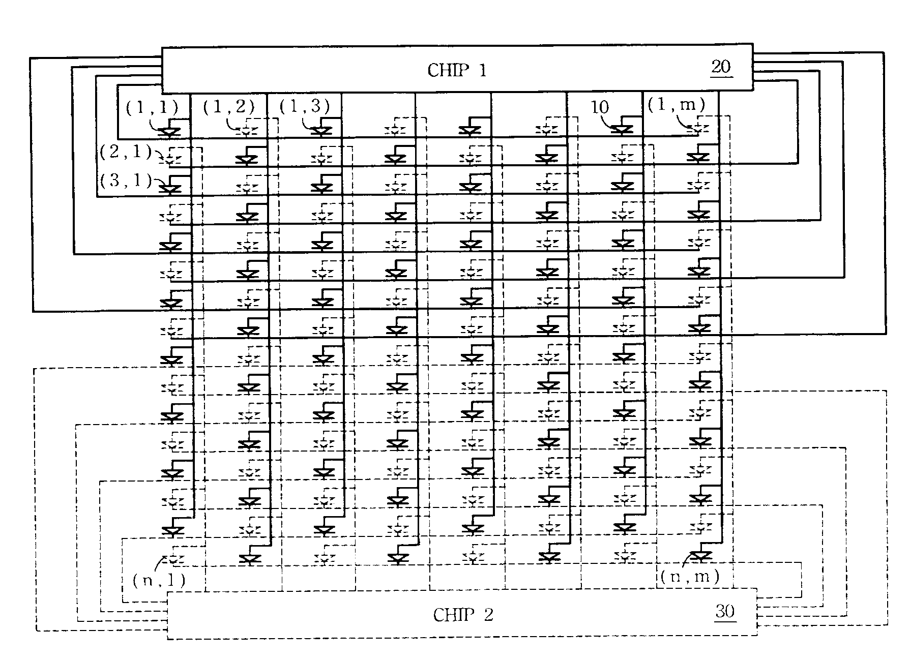
[0028]FIG. 3 illustrates a schematic circuit diagram according to a first embodiment of the present invention. In this embodiment, pixels in the array are alternatively connected and driven by the first driving chip 20 and the second driving chip 30. Each of the pixels contains an OLED 10.

[0029]In FIG. 3 the pixel at the intersection of the first row line and the first column line (the upper le...


PUM


Abstract

A luminescent display device is disclosed. The luminescent display device is comprised of an array of pixels, a first driving chip and a second driving chip. The array of pixels is comprised of columns and rows of pixels. The first driving chip is connected a first pixel of the array of pixels, and the second driving chip is connected to a second pixel of the array of pixels. The second pixel is adjacent to the first pixel. The first driving chip is not connected to all pixels in a row of the at least one row of pixels.

Description

BACKGROUND OF THE INVENTION[0001]1. Field of the Invention[0002]The present invention generally relates to a circuit for driving an organic light emitting diode (hereinafter referred to as β€œOLED”) display, and in particular certain embodiments of the present invention relate to a dual-scan circuit for driving an OLED display device.[0003]2. Description of the Related Art[0004]An OLED display device is an electro-luminescence device. Generally, an OLED display device is made of a stack of layers on a glass substrate. The stack of layers is generally formed by an anode electrode, a hole-injection layer, a light-emitting layer, an electron-injection layer, and a cathode electrode in sequence. The anode electrode is an electrically conductive material formed and patterned on the glass substrate.[0005]When a current source is applied to the OLED display device, there is an electric potential difference between the anode electrode and the cathode electrode. The holes in the hole-injection...

Claims


Application Information

Patent Timeline
27 Dec 2007
Publication
US20070296650A1
IPC
G09G3/30
CPC
G09G3/3216; G09G2310/0278; G09G2310/0221
Inventors
CHANG, CHIN-TIEN