Array substrate for liquid crystal display device and method of fabricating the same

a liquid crystal display and substrate technology, applied in non-linear optics, instruments, optics, etc., can solve the problems of reduced aperture ratio, increased common line b>40/b>, and difficulty in controlling the liquid crystal corresponding to the common line b, so as to reduce signal distortion, reduce light leakage, and improve contrast ratio

Inactive Publication Date: 2007-12-27
LG DISPLAY CO LTD
View PDF9 Cites 19 Cited by
  • Summary
  • Abstract
  • Description
  • Claims
  • Application Information

AI Technical Summary

Benefits of technology

[0021]An object of the present invention is to provide an array substrate for an LCD device and a method of fabricating the same wherein the contrast ratio is improved by reducing the signal distortion between the common line and the pixel electrode and by reducing the light leakage.
[0022]Another object of the present invention is to provide an array substrate for an ...

Problems solved by technology

However, there are problems including an interference problem due to coupling of the gate signal.
However, the aperture ratio is reduced due to a light leakage.
Therefore, it is difficult to control the liquid crystal corresponding to the common line 40 and the pixel electrode 60.
Furthermore, if the aperture ...

Method used


Image

  • Array substrate for liquid crystal display device and method of fabricating the same
  • Array substrate for liquid crystal display device and method of fabricating the same
  • Array substrate for liquid crystal display device and method of fabricating the same

Examples


Embodiment Construction

[0036]Reference will now be made in detail to the preferred embodiments of the present invention, examples of which are illustrated in the accompanying drawings.

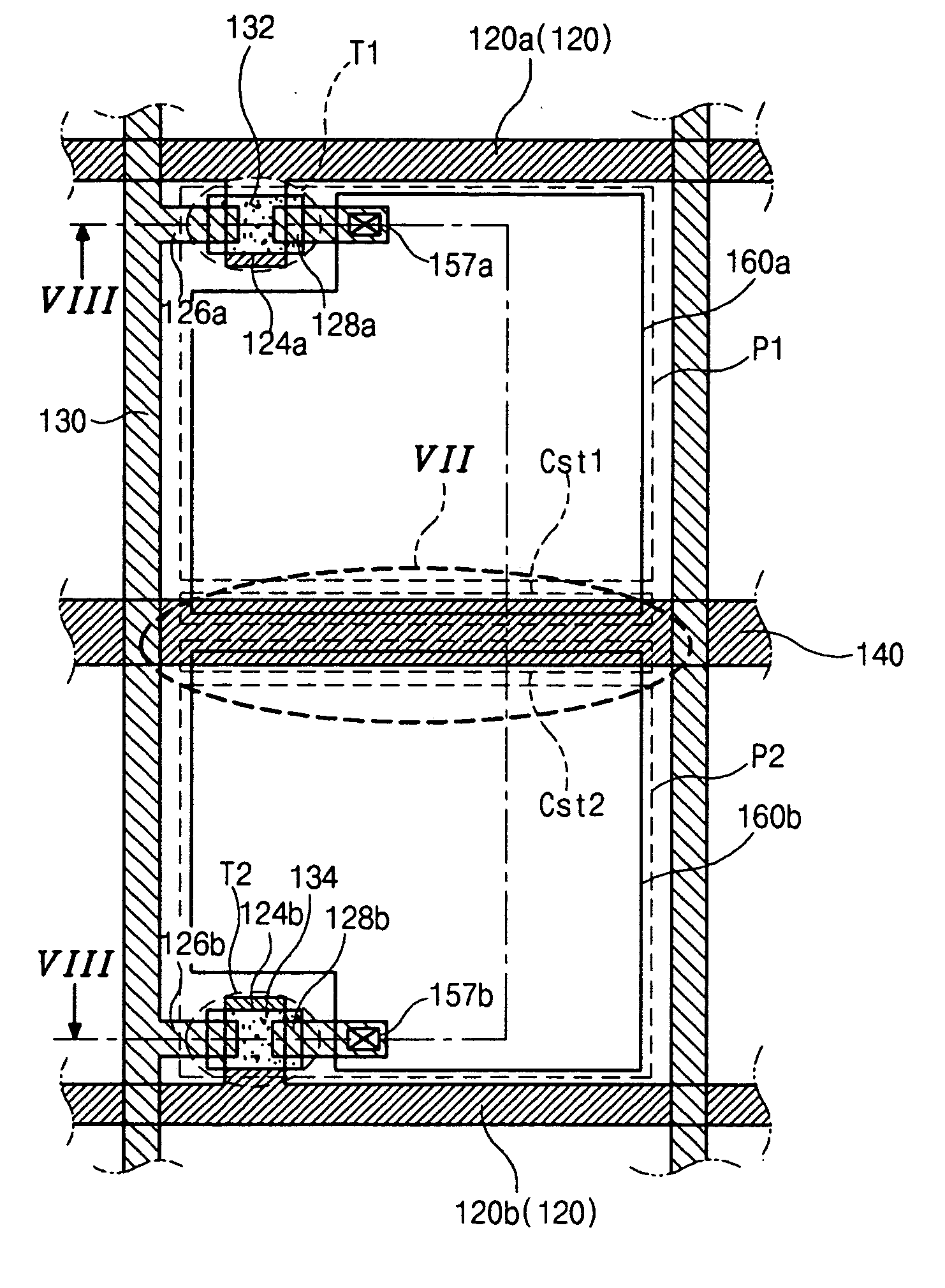
[0037]FIG. 5 is a schematic plan view of an array substrate for an LCD device according to an exemplary embodiment of the present invention, FIG. 6 is an exploded view of two pixel regions of a region “VI” of FIG. 5 according to the exemplary embodiment of the present invention, and FIG. 7 is an exploded view of a region “VII” of FIG. 6 according to the exemplary embodiment of the present invention. In FIGS. 5, 6, and 7, a plurality of gate lines 120 are formed along a first direction on a substrate 100, and a plurality of data lines 130 are formed along a second direction crossing the second direction. The gate lines 120 include first and second gate lines 120a and 120b spaced apart from each other. A first gate electrode 124a extends from the first gate line 120a, and a second gate electrode 124b extends from the second ga...


PUM


Abstract

An array substrate for liquid crystal display devices includes first and second gate lines spaced apart from each other, a common line between the first and second gate lines parallel to the first and second gate lines, a data line crossing the first and second gate lines to define first and second pixel regions with respect to the common line, a first thin film transistor at a crossing portion of the first gate line and the data line, a second thin film transistor at a crossing portion of the second gate line and the data line, a first pixel electrode connected to the first thin film transistor in the first pixel region, and a second pixel electrode connected to the second thin film transistor in the second pixel region, wherein the first and second pixel electrodes have a symmetric shape with respect to the common line.

Description

[0001]The present invention claims the benefit of Korean Patent Application No. 10-2006-058231, filed in Korea on Jun. 27, 2006, which is hereby incorporated by reference.BACKGROUND OF THE INVENTION[0002]1. Field of the Invention[0003]The present invention relates to a liquid crystal display (LCD) device, and more particularly, to an array substrate for an LCD device that has a high aperture and a method of fabricating the same.[0004]2. Discussion of the Related Art[0005]Generally, an LCD device uses optical anisotropy and the polarization properties of liquid crystal molecules to display images. Liquid crystal molecules that are thin and long have directionality. The alignment direction of the liquid crystal molecules may be controlled by applying an electric field to the liquid crystal molecules. As the intensity of the electric field changes, the alignment of the liquid crystal molecules changes accordingly. Because the refraction of the incident light through liquid crystals dep...

Claims


Application Information

Patent Timeline
IPC IPC(8): G02F1/136
CPCG02F1/136286G02F2201/40G02F2001/134345G02F1/134345G02F1/136
Inventor KWON, KI-YOUNGHWANG, KWANG-HEE
Owner LG DISPLAY CO LTD
Why Eureka
Try Eureka