Array substrate for in-plane switching mode liquid crystal display device and method of fabricating the same

a liquid crystal display and in-plane switching technology, applied in non-linear optics, instruments, optics, etc., can solve the problems of reducing production yield, bad viewing angle of am-lcd devices, and repairing disconnected data lines

Active Publication Date: 2007-12-27
LG DISPLAY CO LTD
View PDF5 Cites 49 Cited by
  • Summary
  • Abstract
  • Description
  • Claims
  • Application Information

AI Technical Summary

Benefits of technology

[0013]Accordingly, the present invention is directed to an array substrate for an IPS mode LCD device and a method of fabrication the same that substantially obviates one or more of the problems due to limitations and disadvantages of the related art.

Problems solved by technology

However, since the AM-LCD device uses a vertical electric field, the AM-LCD device has a bad viewing angle.
However, there are some limitations.
Particularly, when an electric line, e.g., the data line, is disconnected during a fabricating process, it is difficult to repair the disconnected data line and thus, the production yield is reduced.
Furthermore, since a magnitude of the electric field between the common electrode and the pixel electrode decreases due to the gate insulating layer and the passivation layer, power consumption increases.

Method used


Image

  • Array substrate for in-plane switching mode liquid crystal display device and method of fabricating the same
  • Array substrate for in-plane switching mode liquid crystal display device and method of fabricating the same
  • Array substrate for in-plane switching mode liquid crystal display device and method of fabricating the same

Examples


first embodiment

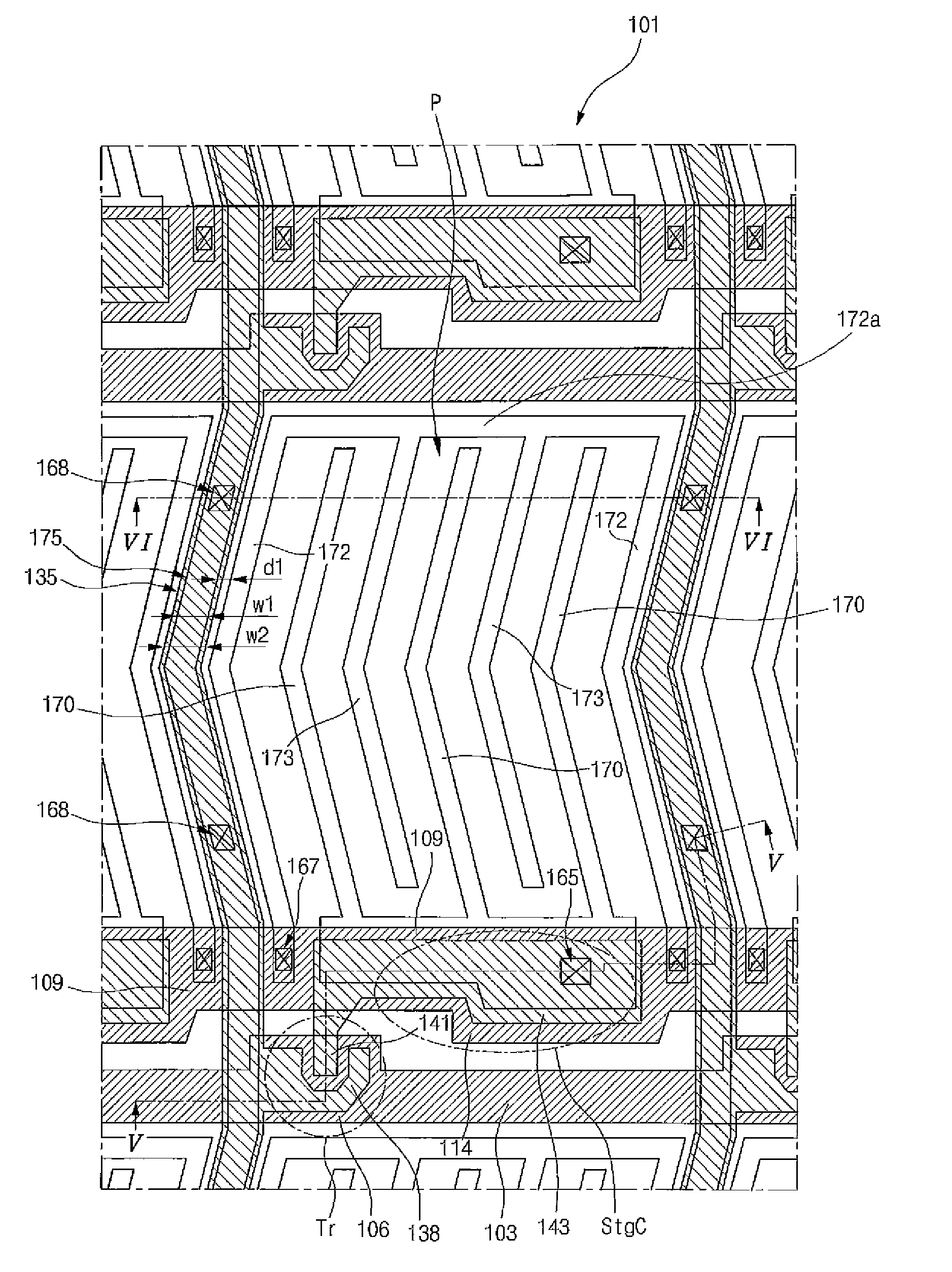
[0033]FIG. 4 is a plane view showing an array substrate for an IPS mode LCD device according to the present invention. As shown in FIG. 4, a gate line 103 and a data line 135 are formed on a substrate 101. The gate line 103 and the data line 135 cross each other to define a pixel region P. A common line 109 is formed on the substrate lot. The common line 109 is substantially parallel to and spaced apart from the gate line 103. A TFT Tr including a gate electrode 106, a gate insulating layer (shown in FIG. 5), a semiconductor layer (shown in FIG. 5), a source electrode 138 and a drain electrode 141 is formed at crossing of the gate and data lines 103 and 135. A gate electrode 106 is connected to the gate line 103, and the gate insulating layer is formed on the gate electrode 106. The gate electrode 106 may be a portion of the gate line 103. The semiconductor layer is formed on the gate insulating layer and corresponds to the gate electrode 106. The source and drain electrodes 138 and...

second embodiment

[0051]Moreover, in the array substrate for the IPS mode LCD device according to the present invention, since the auxiliary data line 275 is disposed over and connected to the data line 235, the TFT Tr can receive the signal due to the auxiliary data line 275 when the data line 235 disconnected. Namely, the auxiliary data line 275 functions as a self-repairing line, which is advantageous.

[0052]Furthermore, since the plurality of pixel electrodes 270 and the second common electrodes 273 are formed on the same level, a perfect horizontal electric field is generated between the pixel electrode 270 and the second common electrode 273 such that the IPS mode LCD device displays improved images. In addition, since there is no insulating layer, for example, a gate line and a passivation layer, between the second common electrodes and the pixel electrodes, power consumption decreases.

[0053]Methods for fabricating the array substrates of the first and second embodiments are discussed. Particul...


PUM

PropertyMeasurementUnit
widthaaaaaaaaaa
optical anisotropyaaaaaaaaaa
electric fieldaaaaaaaaaa

Abstract

An array substrate for an in-plane switching mode liquid crystal display device and its fabrication method are discussed. According to an embodiment, the array substrate includes a gate line and a data line crossing the gate line on a base substrate, so as to define a pixel region; a thin film transistor connected to the gate line and the data line; a plurality of pixel electrodes disposed in the pixel region and connected to the thin film transistor; a common line extending substantially parallel to the gate line; and a plurality of common electrodes alternately arranged with the plurality of pixel electrodes in the pixel region, wherein the plurality of common electrodes include at least one first common electrode adjacent to the data line and connected to the common line, and at least one second common electrode extending substantially parallel to the date line and not directly connected to the common line.

Description

[0001]The present application claims the priority benefit of Korean Patent Application No. 10-2006-0055781 filed in Korea on Jun. 21, 2006, which is hereby incorporated by reference.BACKGROUND OF THE INVENTION[0002]1. Field of the Invention[0003]The present invention relates to an array substrate for an in-plane switching (IPS) mode liquid crystal display (LCD) device and more particularly to an array substrate for an IPS mode LCD device having a repair pattern and a method of fabrication the array substrate.[0004]2. Discussion of the Related Art[0005]A related art liquid crystal display (LCD) device uses optical anisotropy and polarization properties of liquid crystal molecules. The liquid crystal molecules have a definite alignment direction as a result of their thin and long shapes. The alignment direction of the liquid crystal molecules can be controlled by applying an electric field across the liquid crystal molecules. In other words, as the intensity or direction of the electr...

Claims


Application Information

Patent Timeline
Patent Type & Authority Applications(United States)
IPC IPC(8): G02F1/1343
CPCG02F1/134363G02F2001/136272G02F2001/136263G02F1/136259G02F1/136263G02F1/136272G02F1/1343
Inventor SEO, BUM-SIKKIM, JI-WON
Owner LG DISPLAY CO LTD
Why Eureka
Try Eureka