Junction field effect thin film transistor

a junction field effect and transistor technology, applied in the direction of transistors, semiconductor devices, electrical devices, etc., can solve the problems of deteriorating the properties of conventional tft, increasing power consumption, etc., and achieve the effect of reducing the mobility of carriers

Active Publication Date: 2008-01-03
SAMSUNG ELECTRONICS CO LTD
View PDF6 Cites 13 Cited by
  • Summary
  • Abstract
  • Description
  • Claims
  • Application Information

AI Technical Summary

Benefits of technology

[0012]Example embodiments are directed to a junction field effect thin film transistor (JFETFT) that can solve a decrease in the mobility of carriers of the conventional TFT.

Problems solved by technology

However, when a portion of the semiconductor layer 30 that may be adjacent to the gate insulating layer 25 may be used as a channel in the conventional TFT, many defects may be present at an interface (portion A) of the gate insulating layer 25 and the semiconductor layer 30, which may result in a decrease in the mobility of carriers.
Also, in the conventional TFT, the gate insulating layer 25 may have to be charged to turn-on the TFT, thereby decreasing the operation speed and increasing power consumption.
Moreover, in order to obtain a high quality gate insulating layer 25, a high temperature process may be required, which may deteriorate the properties of the conventional TFT, and may limit the available types of substrates that may be used.
For example, a plastic substrate may not be used in a TFT manufacturing process that requires a high temperature process.

Method used


Image

  • Junction field effect thin film transistor
  • Junction field effect thin film transistor
  • Junction field effect thin film transistor

Examples


Embodiment Construction

[0028]Embodiments will be described more fully with reference to the accompanying drawings, in which example embodiments are shown. In the drawings, the thicknesses of layers and regions may be exaggerated for clarity.

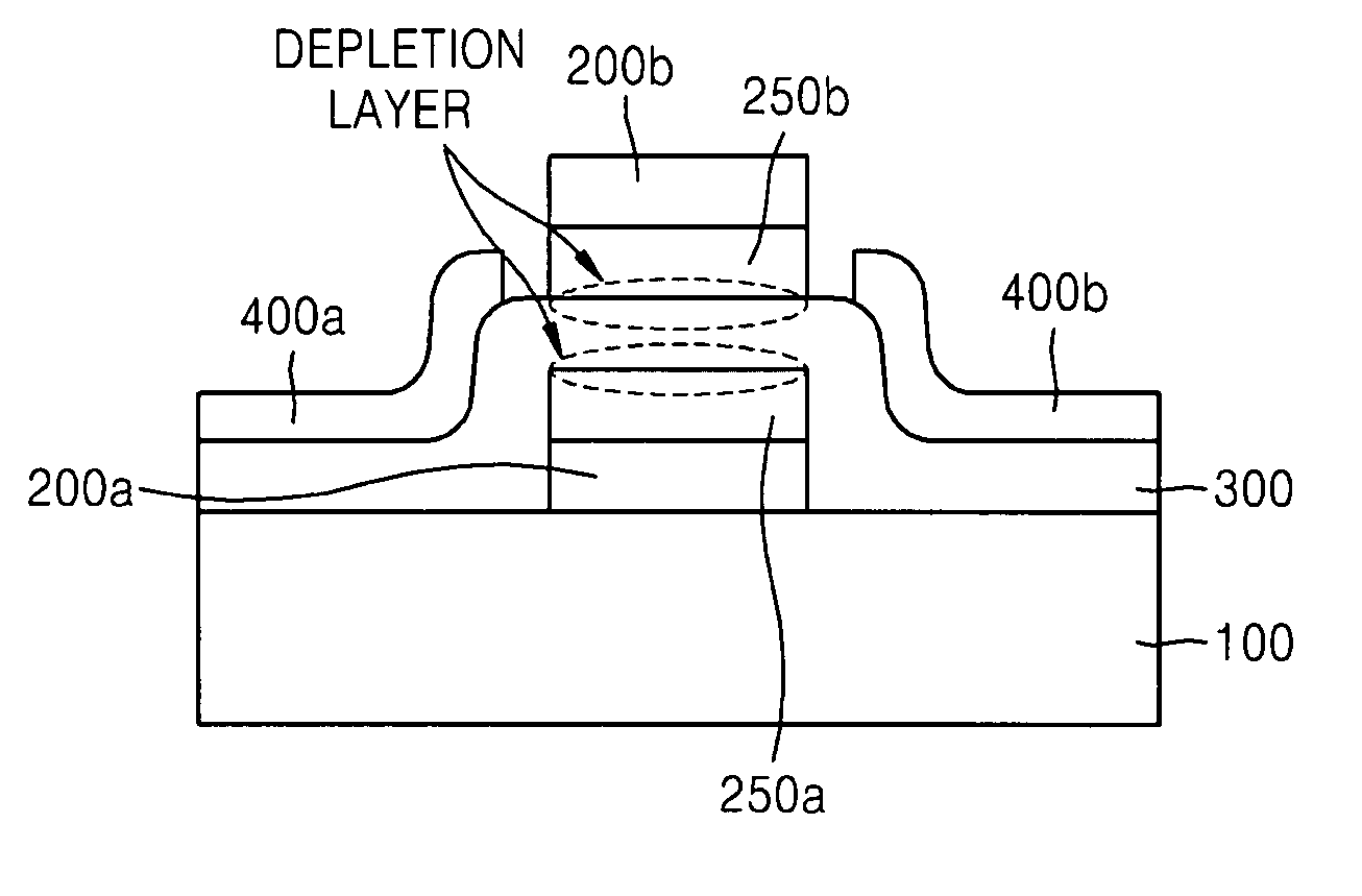
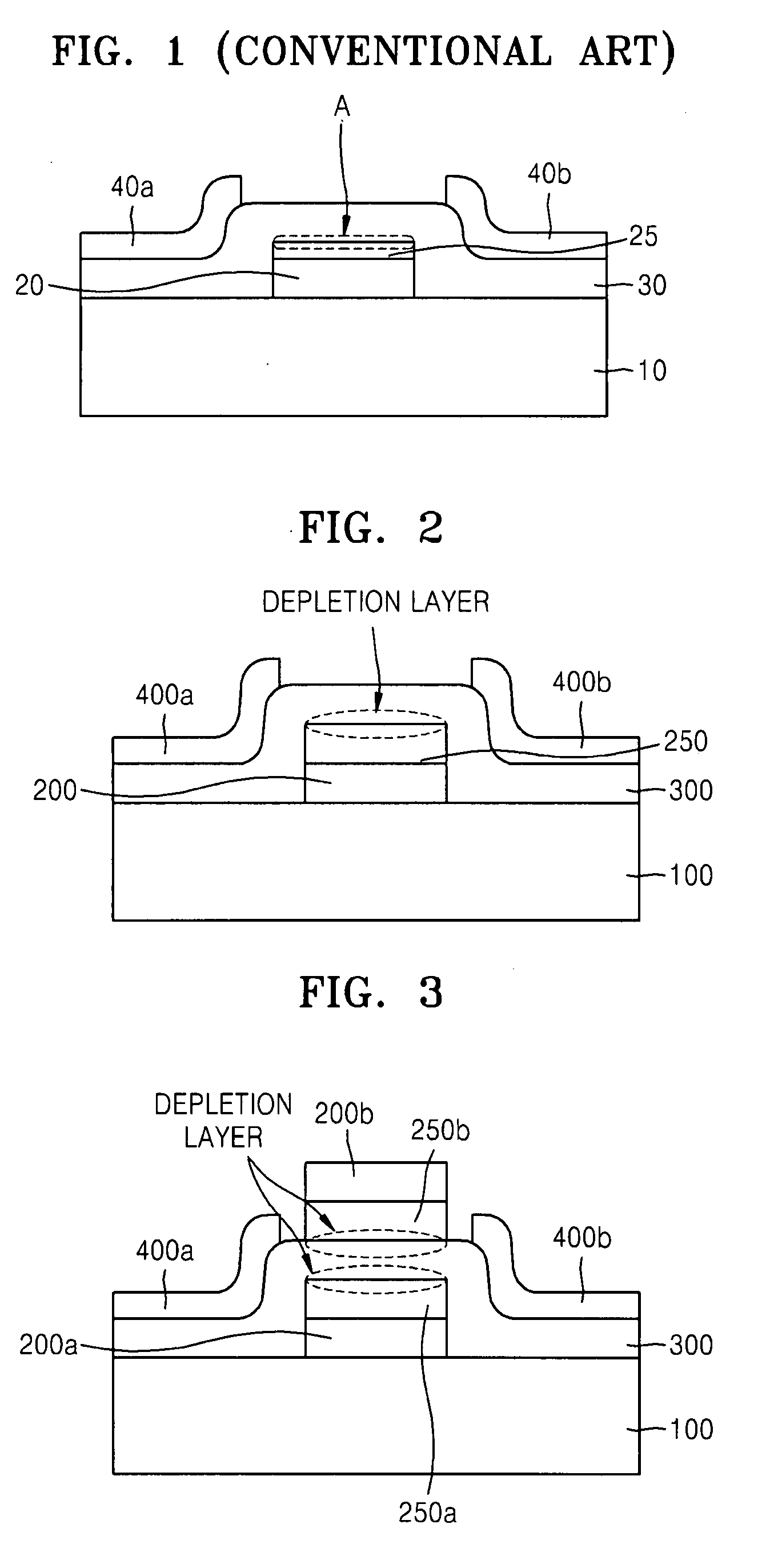
[0029]First, a technical principle will be described briefly. Example embodiments are directed to a junction field effect thin film transistor (JFETFT) which may have a p-n junction, and not a conventional metal oxide semiconductor (MOS) structure. For example, an n-type semiconductor may be used as a semiconductor layer for a channel, a p-type semiconductor may be used as a gate material, and the size of a depletion region generated from junction regions between the materials may be controlled to switch the thin film transistor (TFT) on and off. The channel may be formed inside the semiconductor layer, and not at the interface of the semiconductor layer, and thus the mobility of carriers may be improved as compared to a conventional TFT that may use an interface as a ...


PUM


Abstract

Example embodiments are directed to a junction field effect thin film transistor (JFETFT) including a first electrode formed on a substrate, a first conductive first gate semiconductor pattern formed on the first gate electrode, a second conductive semiconductor channel layer formed on the substrate and the first conductive first gate semiconductor pattern, and source and drain electrodes formed on the second conductive semiconductor pattern and located at both sides of the first conductive gate semiconductor pattern. The JFETFT may further include a first conductive second gate semiconductor pattern formed on a portion of the second conductive semiconductor channel layer between the source electrode and the drain electrode, and a second gate electrode formed on the first conductive second gate semiconductor pattern.

Description

PRIORITY STATEMENT[0001]This application claims the benefit of Korean Patent Application No. 10-2006-0058893, filed on Jun. 28, 2006 in the Korean Intellectual Property Office, the disclosure of which is incorporated herein in its entirety by reference.BACKGROUND[0002]1. Field[0003]Example embodiments relate to a thin film transistor (TFT), and more particularly to a junction field effect TFT.[0004]2. Description of the Related Art[0005]A thin film transistor (TFT) may be a switching device used, for example, in liquid crystal display devices, in organic electroluminescent (EL) display devices, or in memory devices, and may generally have a metal oxide semiconductor field effect transistor (MOSFET) structure as illustrated in FIG. 1.[0006]Referring to FIG. 1, a conventional TFT may include a predetermined or given substrate 10, for example, silicon, on which a gate electrode 20 and a gate insulating layer 25 may be sequentially formed. A semiconductor layer 30 may be formed on the g...

Claims


Application Information

Patent Timeline
Patent Type & Authority Applications(United States)
IPC IPC(8): H01L29/80
CPCH01L29/8086H01L29/66901H01L29/4908H01L29/78648H01L29/7869
Inventor GENRIKH, STEFANOVICHCHO, CHOONG-RAELEE, EUN-HONG
Owner SAMSUNG ELECTRONICS CO LTD
Why Eureka
Try Eureka