Power amplifier module

a technology of power amplifier and module, which is applied in the field of power amplifier modules, can solve the problems of difficult insertion of power amplifier chips, difficult to meet this demand, and the size of power amplifier modules of 3 mm3 mm is barely capable of being achieved with the conventional implementation, so as to achieve the effect of reducing the volum

Inactive Publication Date: 2008-01-03
NEC ELECTRONICS CORP
View PDF4 Cites 17 Cited by
  • Summary
  • Abstract
  • Description
  • Claims
  • Application Information

AI Technical Summary

Benefits of technology

[0022]In accordance with the present invention, it is possible to realize a miniaturized IC module, e.g., power amplifier module that was difficult to achieve by an extension of the prior art.
[0023]Further, in accordance with the present invention (third to fourth aspects), cavity volume can be reduced and a bonding area is no longer necessary. This makes further miniaturization possible.

Problems solved by technology

A power amplifier module having a size of 3 mm×3 mm is barely capable of being achieved with the conventional implementation.
It is likely that there will be increasing demand for further miniaturization in the coming years and it is believed that meeting this demand will be difficult merely by an extension of conventional methods of manufacture.
However, since an output matching circuit, which has a major influence upon the characteristics of the power amplifier, requires a certain degree of line length, incorporating it in the power amplifier chip is difficult and therefore it is necessary to form the circuit externally.
The LTCC wiring board, however, uses up most of the area of the power amplifier chip.
This means that area available within the LTCC for fabricating the matching circuit is small.

Method used


Image

  • Power amplifier module
  • Power amplifier module
  • Power amplifier module

Examples


first example

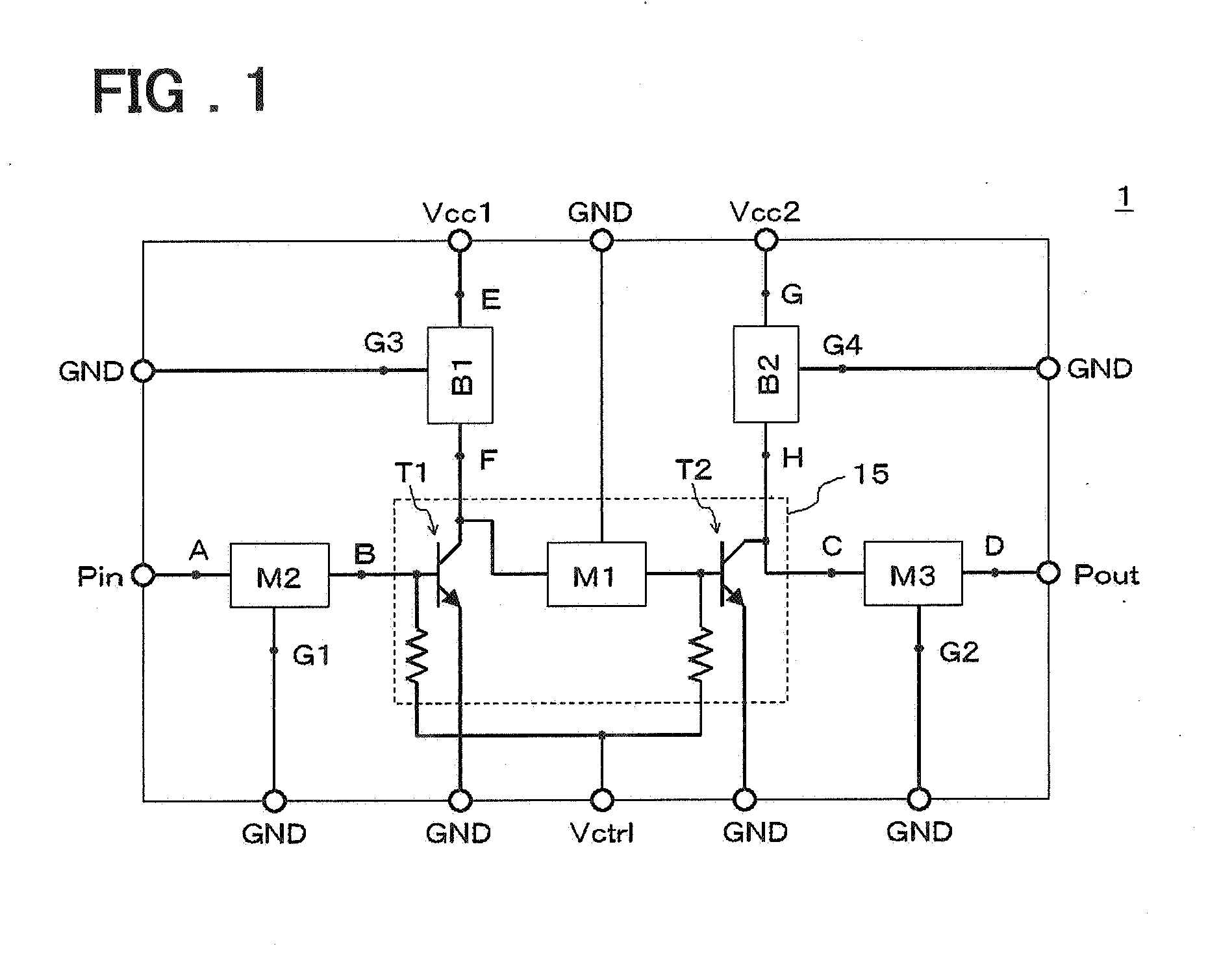
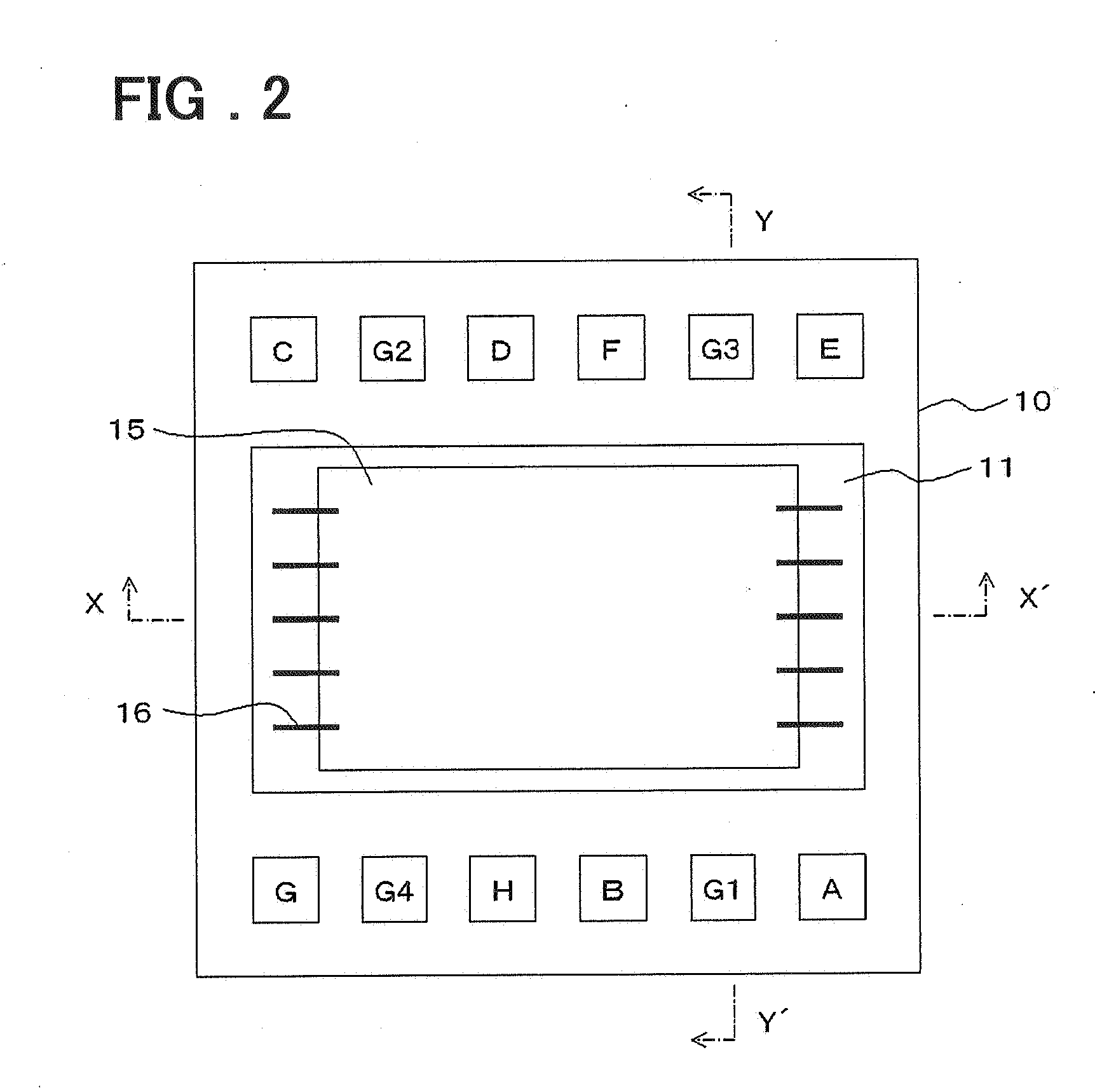
[0032]A power amplifier module according to a first example of the present invention will be described with reference to the drawings, in which FIG. 1 is a block diagram schematically illustrating a power amplifier module 1 according to the first example, exemplified as an IC module of a stacked structure.

[0033]The power amplifier module 1 depicted in FIG. 1 is indicative of a two-stage amplifier. The power amplifier module 1 has a power amplifier chip 15, an input matching circuit M2, an output matching circuit M3, a bias circuit B1 and a bias circuit B2.

[0034]The power amplifier chip 15 includes an interstage matching circuit M1 connected between an initial-stage transistor T1 and a final-stage transistor T2. The transistor T1 is constituted by a GaAsHBT or the like, e.g., and has a collector electrically connected to the interstage matching circuit M1 and to bias circuit B1, a base electrically connected to the input matching circuit M2 and electrically connected to a control pad...

second example

[0049]A power amplifier module according to a second example of the present invention will now be described. In the power amplifier module according to the second example, the connection between the first LTCC wiring board and the power amplifier chip uses bump-joining instead of bonding wire. As a result, the volume of the cavity can be reduced, a bonding area is no longer necessary and further miniaturization can be achieved.

third example

[0050]A power amplifier module according to a third example of the present invention will now be described. In the power amplifier module according to the third example, the power amplifier chip is made one in which a via is provided below the bonding pad and a pad corresponding to this via is provided on the reverse side (underside) of the chip. The power amplifier chip is bump-joined to the first LTCC wiring board. As a result, the volume of the cavity can be reduced, a bonding area is no longer necessary and further miniaturization can be achieved.

[0051]As many apparently widely different modes or examples of the present invention can be made without departing from the spirit and scope thereof, it is to be understood that the invention is not limited to the specific examples thereof except as defined in the appended claims.

[0052]In a further aspect, the IC module of a stacked layer structure comprises a first wiring board and a second wiring board wiring board, each of which may ...


PUM


Abstract

A power amplifier module (IC module) of stacked layer structure is miniaturized while dissipating heat from a power amplifier chip. The module includes a first LTCC wiring board having a cavity in which a power amplifier chip is embedded, and a plurality of vias, which are electrically connected to ground, immediately underlying the power amplifier chip; and a second LTCC wiring board joined to the first LTCC wiring board and incorporating a matching circuit and a bias circuit electrically connected to the power amplifier chip. Ground pads of the matching circuit and bias circuit are all grounded by separating wiring or vias in the first LTCC wiring board and second LTCC wiring board.

Description

RELATED APPLICATION[0001]This application is based upon and claims the benefit of the priority of Japanese patent application No. 2006-178, filed on Jun. 28, 2006, the disclosure of which is incorporated herein in its entirety by reference thereto.FIELD OF THE INVENTION[0002]This invention relates to an IC module having a plurality of wiring boards of a stacked structure, particularly, a power amplifier module those employing ceramic wiring boards, typically, LTCC (Low-Temperature Co-fired Ceramic) wiring boards. More particularly, the invention relates to a power amplifier module that enables miniaturization.BACKGROUND OF THE INVENTION[0003]Power amplifier modules for WCDMA (Wideband Code Division Multiple Access) currently being developed typically have a size of 3 mm×3 mm. As illustrated in FIGS. 6A to 6C, a power amplifier module having a size of 3 mm×3 mm comprises a power amplifier chip 101 constituted by a GaAsHBT (GaAs heterojunction bipolar transistor) or the like; an LTCC ...

Claims


Application Information

Patent Timeline
Patent Type & Authority Applications(United States)
IPC IPC(8): H01L23/15
CPCH01L25/16H03F3/189H05K1/0306H05K1/144H05K1/183H01L2224/49175H01L2224/48091H01L2224/45144H01L2924/1305H01L2924/3011H01L2924/00014H01L2924/00H01L2924/30111
Inventor NISHIMURA, YOSHIKAZUGOTO, KEIZO
Owner NEC ELECTRONICS CORP
Why Eureka
Try Eureka