GaN Compound Semiconductor Light Emitting Element and Method of Manufacturing the Same

a technology of compound semiconductor and light-emitting element, which is applied in the direction of semiconductor/solid-state device manufacturing, semiconductor devices, electrical devices, etc., can solve the problems of complex manufacturing process, degraded optical output, and inability to be smoothly removed, so as to achieve easy chip separation

Active Publication Date: 2008-01-10
SEOUL VIOSYS CO LTD +1
View PDF5 Cites 82 Cited by
  • Summary
  • Abstract
  • Description
  • Claims
  • Application Information

AI Technical Summary

Benefits of technology

[0004] Therefore, the present invention is conceived to solve the above problems. An object of the present invention is to provide a gallium nitride (GaN) compound semi-conductor light emitting element (LED) and a method of manufacturing the same, in which a multi-layered metallic support is formed underside a vertical GaN LED to thereby enable an easy chip separation, and an insulation film and metallic protective film layer are sequentially formed on a lateral surface of the element to thereby enable the protection of an epitaxially grown GaN substrate.
[0006] A further object of the present invention is to provide a GaN compound semi-conductor LED and a method of manufacturing the same, in which a metallic substrate, conductive layer substrate or conductive ceramic substrate is used, instead of a sapphire substrate, to efficiently release heat generated upon the operation of the element to the outside, so that the LED can be suitable for a high-power application.
[0007] A still further object of the present invention is to provide a GaN compound semi-conductor LED and a method of manufacturing the same, in which photons generated in an InGaN layer are emitted through an n-GaN layer to provide a short path to the photons, so that the number of photons absorbed while being emitted can be reduced.

Problems solved by technology

In such a case, when it is in a high-power operation, the current spreading-resistance is high, and thus, its optical output is degraded.
In addition, heat generated when the element is operated cannot be smoothly removed and thus thermal stability of the element is degraded to thereby cause a problem related with the high-power operation.
However, since the flip-chip structure must be packed in the form of a flip-chip, the manufacturing process is complicated.

Method used


Image

  • GaN Compound Semiconductor Light Emitting Element and Method of Manufacturing the Same
  • GaN Compound Semiconductor Light Emitting Element and Method of Manufacturing the Same
  • GaN Compound Semiconductor Light Emitting Element and Method of Manufacturing the Same

Examples


first embodiment

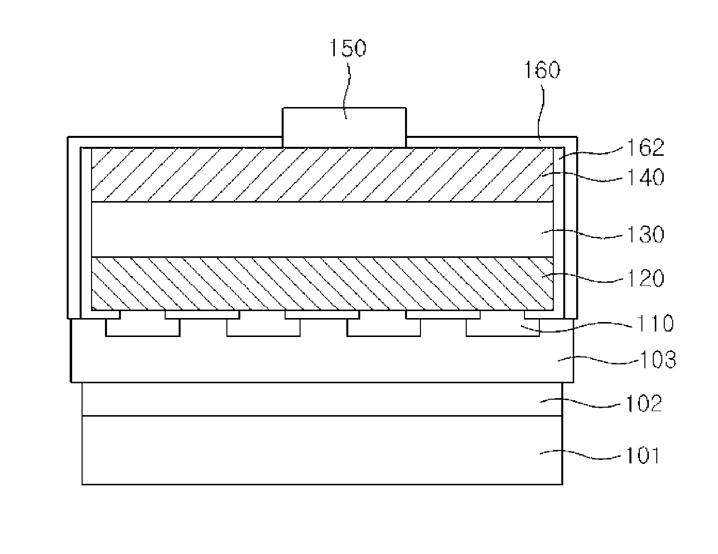
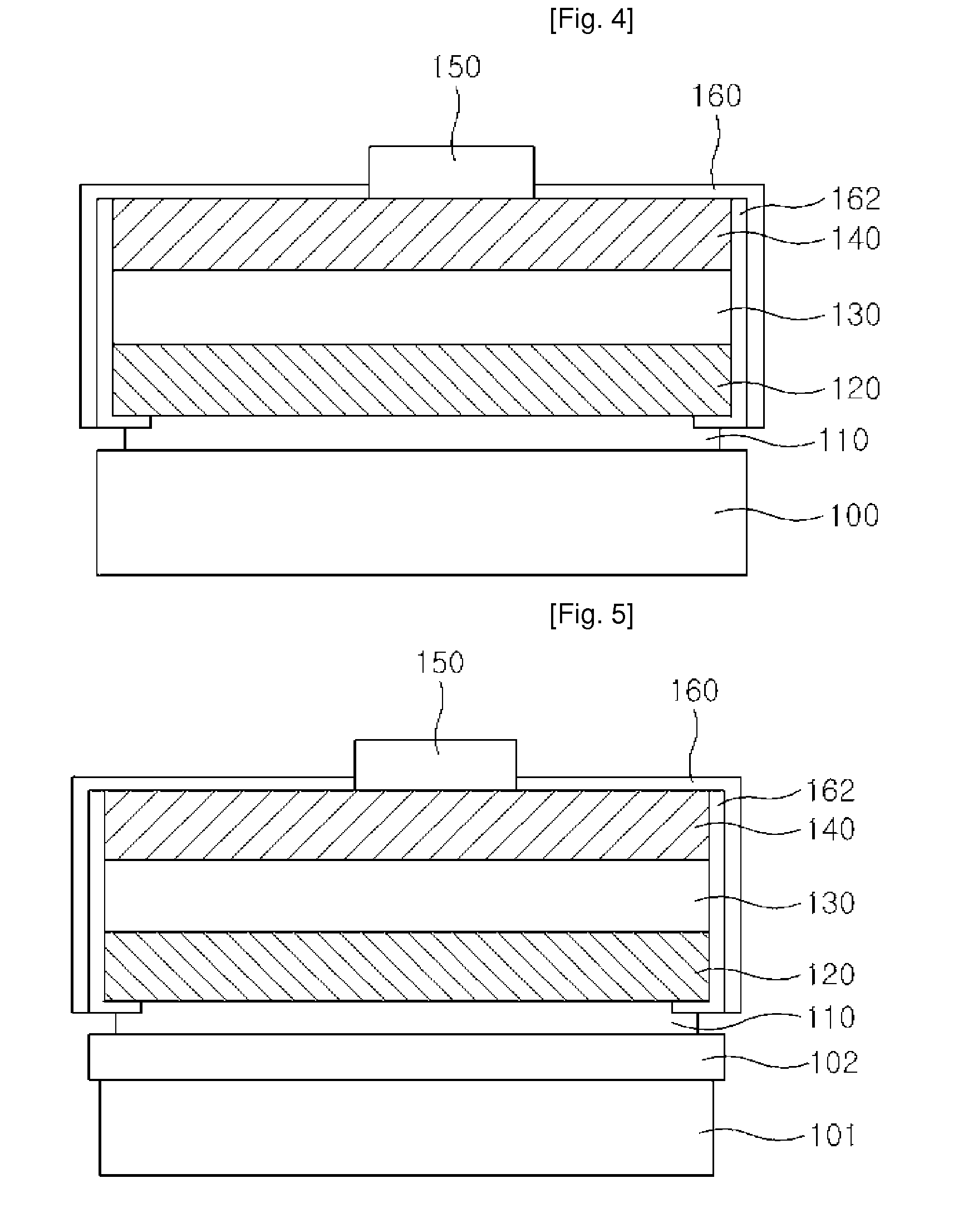
[0047]FIG. 4 is a sectional view of a vertical LED according to the present invention, and FIGS. 5 to 7 are sectional views of a vertical LED according to a modified embodiment of the present invention.

[0048] As shown in FIG. 4, the vertical GaN LED of this embodiment includes a metallic support layer 100, a reflective film electrode 110 (a p-type reflective film ohmic electrode layer), a p-type semiconductor layer 120, an InGaN active layer 130 and an n-type semiconductor layer 140 in sequence from the bottom.

[0049] Referring to FIG. 5, a vertical GaN LED according to a modified embodiment of the present invention employs a double-layered metallic support composed of first and second metallic support layer 101 and 102 to enable easy chip separation. In a vertical GaN LED shown in FIG. 6, a p-type reflective film electrode 110 is partially formed on a p-type semiconductor in a mesh form and a reflective layer 103 is then inserted therebetween, so that light generated in the i-InGaN...

second embodiment

[0092] The present invention is not limited to the foregoing. For example, the epitaxially grown GaN substrate can be protected by forming an insulation film on a lateral surface of the element and then coating a metallic protective film layer on a top surface of the P-type electrode and the lateral surface of the element. Hereinafter, a vertical LED having a metallic protective film layer according to the present invention will be described.

[0093]FIG. 53 is a sectional view of a vertical LED according to the second embodiment of the present invention. FIGS. 54 to 58 are sectional views of a vertical LED according to modified embodiments of the present invention.

[0094] Referring to FIG. 53, the vertical GaN LED is configured in such a manner that an insulation film 1700 is first coated on the lateral surface of the element composed of a P-type semiconductor layer 1300, an active layer 1400 and an N-type semiconductor layer 1500, and a metallic protective film layer 1100 is then coa...


PUM

PropertyMeasurementUnit
thicknessaaaaaaaaaa
total thicknessaaaaaaaaaa
thicknessaaaaaaaaaa

Abstract

The present invention relates to a gallium nitride (GaN) compound semiconductor light emitting element (LED) and a method of manufacturing the same. The present invention provides a vertical GaN LED capable of improving the characteristics of a horizontal LED by means of a metallic protective film layer and a metallic support layer. According to the present invention, a thick metallic protective film layer with a thickness of at least 10 microns is formed on the lateral and / or bottom sides of the vertical GaN LED to protect the element against external impact and to easily separate the chip. Further, a metallic substrate is used instead of a sapphire substrate to efficiently release the generated heat to the outside when the element is operated, so that the LED can be suitable for a high-power application and an element having improved optical output characteristics can also be manufactured. A metallic support layer is formed to protect the element from being distorted or damaged due to impact. Furthermore, a P-type electrode is partially formed on a P—GaN layer in a mesh form to thereby maximize the emission of photons generated in the active layer toward the N—GaN layer.

Description

TECHNICAL FIELD [0001] The present invention relates to a gallium nitride (GaN) based blue light emitting diode (LED) and a method of manufacturing the same. More particularly, the present invention relates to a vertical GaN LED element and a method of manufacturing the same. BACKGROUND ART [0002] Recently, the LED using a GaN semiconductor has been predominantly expected to replace existing light sources such as incandescent lamps, fluorescent lamps and mercury lamps. Thus, researches on a high-power GaN LED have been intensively made. In general, a substrate used for manufacturing a GaN LED is configured in such a manner that an n-type GaN 12, undoped InGaN (an active layer; 14) and a p-type GaN 16 are sequentially grown on a sapphire substrate 10, as shown in FIG. 1. Since the sapphire substrate 10 is non-conductive, the LED element typically has a horizontal structure as shown in FIG. 2. Here, reference numerals 18, 20, 22 and 24 denote a P-type transparent electrode, a P-type p...

Claims


Application Information

Patent Timeline
Patent Type & Authority Applications(United States)
IPC IPC(8): H01L33/00H01L21/00H01L33/10H01L33/32H01L33/38H01L33/40H01L33/44
CPCH01L33/0079H01L33/32H01L33/44H01L33/40H01L33/405H01L33/387H01L33/0093
Inventor LEE, JONG LAM
Owner SEOUL VIOSYS CO LTD
Why Eureka
Try Eureka