Semiconductor Device

a technology of semiconductor chips and semiconductor chips, applied in the direction of instruments, heat measurement, basic electric elements, etc., can solve the problems of insufficient temperature measurement accuracy, minute electric current drowned out by noise, etc., and achieve the effect of accurate monitoring of the temperature of the semiconductor chip, high-quality detection circuits, and no need for measuremen

Active Publication Date: 2008-01-10
MITSUBISHI ELECTRIC CORP
View PDF3 Cites 14 Cited by
  • Summary
  • Abstract
  • Description
  • Claims
  • Application Information

AI Technical Summary

Benefits of technology

[0010] An object of the present invention is to provide a semiconductor device capable of accurately monitoring a temperature of a semiconductor chip even in a noise environment, while not requiring a highly accurate detection circuit.
[0012] According to the aspect of the semiconductor device in the present invention, since a variable resistor element is arranged on an emitter electrode as a heat generation source, the temperature of the semiconductor chip can be detected with high accuracy by detecting a change in resistance of the variable resistor element. Moreover, adoption of a variable resistor element, in which an amount of change in resistance per degree Celsius is large, eliminates the need for a highly accurate detection circuit, and allows highly accurate detection of the temperature of the semiconductor chip even in a noise environment. Furthermore, bonding of the variable resistor element onto a ground electrode leads to reduction in influence exerted by the electric field on the variable resistor element, making it possible to perform highly accurate temperature detection.

Problems solved by technology

There are some cases where the semiconductor device is extremely heavily used, and in such cases, the rising temperature might exceed a threshold limit to cause multifunction of the semiconductor device or lead to damage thereto.
Further, there is a problem in that, since an environment where the semiconductor device is used is a high-noise environment, the minute electric current is drowned out by the noise and the temperature cannot be sufficiently monitored.
Moreover, although the diode temperature sensor can be directly set on the semiconductor chip, this makes variations large and causes a problem in terms of accuracy in temperature measurement.
The IC temperature sensor is accurate in temperature measurement, but cannot be directly set on the semiconductor chip, and hence there is no choice but to measure the temperature via a heat conduction material.
For this reason, heat resistance of the IC temperature sensor in the semiconductor chip becomes a problem, thereby making it difficult also for this sensor to perform accurate temperature measurement.
Since the respective temperature sensors have the problems as thus described, it is difficult for a semiconductor device using either of such temperature sensors to accurately monitor a temperature of a semiconductor chip in a noise environment.

Method used


Image

  • Semiconductor Device
  • Semiconductor Device
  • Semiconductor Device

Examples


embodiment 1

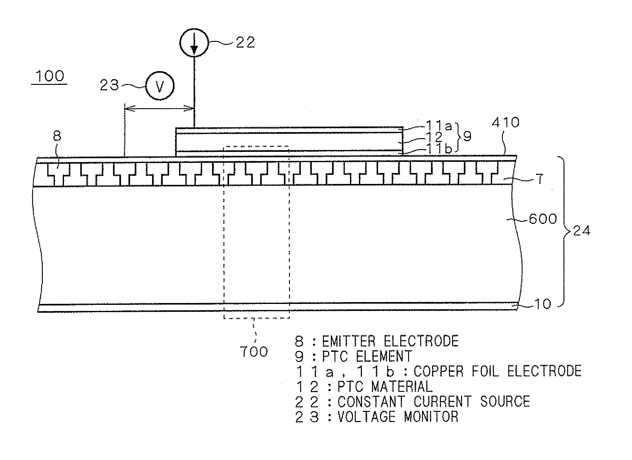
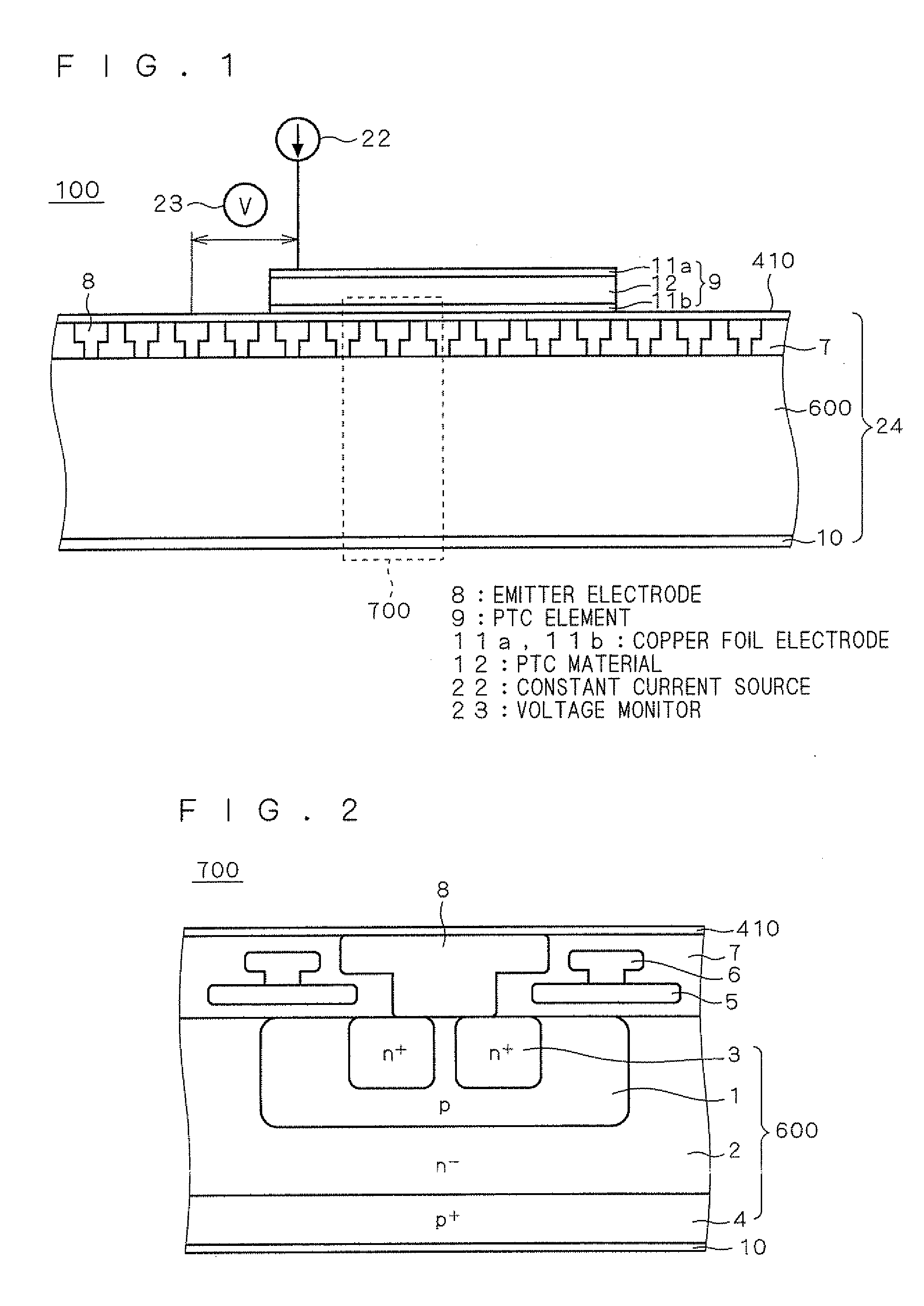
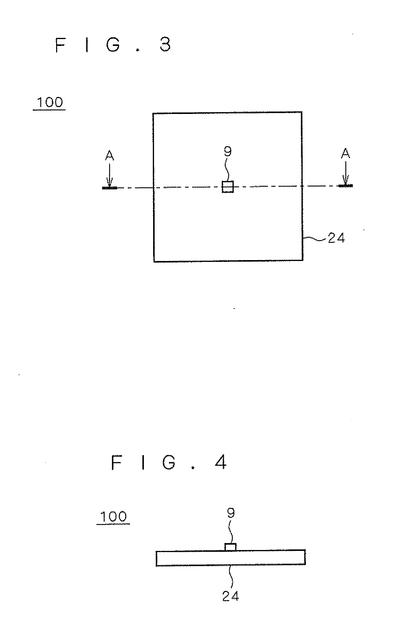
[0031]FIG. 1 is a sectional view showing a configuration of a semiconductor device 100 according to present Embodiment 1. In the semiconductor device 100 according to present Embodiment 1, a PTC (positive temperature coefficient) element (PTC temperature sensor) 9 is bonded to an IGBT (insulated gate bipolar transistor) chip 24 as a kind of semiconductor chips.

[0032] A silicon oxide film 7 is formed on the top surface of a semiconductor layer 600. A plurality of emitter electrodes 8 are formed in the silicon oxide film 7.

[0033] Here, the emitter electrodes 8 are usually connected to a ground potential.

[0034] An aluminum layer 410 for connecting the plurality of emitter electrodes 8 is formed on the emitter electrodes 8. Here, the combination of the plurality of emitter electrodes 8 and the aluminum layer 410 is understood as an emitter-side main electrode.

[0035] A PTC element 9 is bonded onto the aluminum layer 410. The PTC element 9 is a variable resistor element having a posit...

embodiment 2

[0091]FIG. 12 is a sectional view showing a configuration of the vicinity of the PTC element 9 of the semiconductor device 100 according to present Embodiment 2.

[0092] Wires 20, 21 for allowing a current to flow through the PTC element 9 are connected respectively to the copper foil electrodes 11a, 11b of the PTC element 9. A gel (protective film) 15 is then formed so as to cover the PTC element 9.

[0093] The PTC material 12 (see FIG. 1) includes the organic polymer. Therefore, when a transient temperature rise continues, the organic polymer melts, which might cause deformation. Further, the PTC material 12 is vulnerable to moisture, and when the PTC material 12 absorbs moisture, its physical properties may change. Further, it is desirable to avoid damage exerted by mechanical external force.

[0094] In present Embodiment 2, as shown in FIG. 12, the PTC element 9 is covered by the gel 15, for example. This enables prevention of deterioration in characteristic due to absorption of mo...

embodiment 3

[0096] Although the gold bump 14 was used between the copper foil electrodes 11a, 11b of the PTC element 9 and the IGBT chip 24 (see FIG. 10) in present Embodiment 1, the copper foil electrodes 11a, 11b and the surface of the IGBT chip 24 may be directly bonded to each other by the ultrasonic and thermo-compression bonding method without the use of the gold bump 14. Or an Al bump may be used in place of the gold bump 14.

[0097] In present Embodiment 3, the PTC element 9 and the IGBT chip 24 are directly bonded to each other. With the gold bump 14 not used, it is possible to reduce production cost.

[0098] In present Embodiment 3, bonding is performed by the ultrasonic and thermo-compression bonding method. Hence bonding is possible without a temperature rise. Bonding is possible with the surface having been aluminum-deposited or sputtered as often done on the surface of a semiconductor chip, thereby enabling an increase in bonding force.


PUM


Abstract

A semiconductor device accurately monitoring temperature of a semiconductor chip even in a noisy environment, while not requiring a highly accurate detection circuit. A PTC element is bonded onto an IGBT chip. Then, a constant current flows from a constant current source through the PTC element, and an output voltage of the PTC element is detected by a voltage monitor. When output voltage increases, a voltage applied to a gate electrode by a detection circuit is decreased. Since the PTC element is directly arranged on the IGBT chip, the temperature of the IGBT chip can be monitored with high accuracy. Further, since the change in output voltage of the PTC element per 1° C. is large, a highly accurate detection circuit is not necessary, thereby allowing accurate monitoring of the temperature of the IGBT chip even in a noisy environment.

Description

TECHNICAL FIELD[0001] The present invention relates to a semiconductor device including a temperature sensor. BACKGROUND ART [0002] In a semiconductor device as a power device which is in heavy use for power control, a temperature rises with increase in operating current. There are some cases where the semiconductor device is extremely heavily used, and in such cases, the rising temperature might exceed a threshold limit to cause multifunction of the semiconductor device or lead to damage thereto. [0003] Therefore, for example in an invention disclosed in Patent Document 1, a semiconductor device is designed such that a diode temperature sensor is formed inside the semiconductor chip to monitor a temperature of a semiconductor chip, and in the case of detecting an extreme temperature rise, the operation of the semiconductor device is controlled. [0004] Patent Document 1: Japanese Patent Laid-Open No. 2000-31290 [0005] As a conventionally used temperature sensor other than this senso...

Claims


Application Information

Patent Timeline
Patent Type & Authority Applications(United States)
IPC IPC(8): H01L23/34
CPCG01K7/22H01L2924/1305H01L23/34H01L29/7395H01L2224/0401H01L2224/05647H01L2224/48137H01L2924/01012H01L2924/0102H01L2924/01025H01L2924/01057H01L2924/01078H01L2924/01079H01L2924/13055H01L2924/13091H01L2924/3011H01L24/48H01L2924/01019H01L2924/01067H01L23/24H01L2924/1301H01L2924/00H01L2924/19107H01L2224/8592H01L2924/00014H01L2224/48091H01L2224/45099H01L2224/45015H01L2924/207
Inventor INAGUCHI, TAKASHIOHI, TAKESHIFUKUHARA, KATSUHIKOYAMADA, NAOSHIINABA, YOSHITSUGUMITSUHASHI, TAKAO
Owner MITSUBISHI ELECTRIC CORP
Why Eureka
Try Eureka