Build-up printed wiring board substrate having a core layer that is part of a circuit

a technology of build-up and substrate, which is applied in the association of printed circuit non-printed electric components, electrical apparatus construction details, and printed electric component incorporation. it can solve the problems of increasing stress, reducing electrical connection reliability, and reducing so as to reduce the number of resin filled clearance holes, reduce the number of layers, and reduce the thickness of the pwb substrate.

Active Publication Date: 2008-01-17
STABLCOR TECH
View PDF51 Cites 47 Cited by
  • Summary
  • Abstract
  • Description
  • Claims
  • Application Information

AI Technical Summary

Benefits of technology

[0014] In many embodiments, PWB substrates are formed using a build-up micro-wiring structure to create circuits within the PWB substrates that include the core layer. In several embodiments, the core layer forms a power plane, a ground plane or a split power and ground plane. In a number of embodiments, plated through holes are used to establishes electrical connections between the core layer and circuits located on other layers of the PWB substrate. In many embodiments, use of the core as part of the circuit reduces the number of layers required to construct a PWB substrate when compared to an equivalent PWB substrate that includes a core, which is not part of the circuit of the PWB substrate. The elimination of a layer can reduce the thickness of the PWB substrate. In a number of embodiments, use of the core as a ground, power or split plane reduces the number of resin filled clearance holes that are required when compared to a similar PWB substrate design that includes a core layer that does not form part of the PWB substrate circuit.

Problems solved by technology

A problem that can be encountered when using direct die mount with a PWB substrate is that thermal cycling can cause the device to fail.
Therefore, increasing semiconductor die size can cause increased stress on connection points between the semiconductor die and the substrate and ultimately reduce electrical connection reliability.
However, when a larger semiconductor chip is mounted on a substrate, the stress reduction by underfill can be insufficient to ensure reliable contacts between the die pins and the PWB substrate.
Using metals in the construction of a PWB substrate core has a tendency to increase the weight of the PWB substrate compared to the use of a fiberglass based core material.
In addition, thick metal core layers are very difficult to process.
A potential exists, however, for PWB substrates with cores constructed using carbon fiber materials in the manner outlined in the Tani et al. references to fail when there is a high density of plated through holes extending through the core.
Beyond a certain point, the amount of material removed can compromise the physical properties of the core.

Method used


Image

  • Build-up printed wiring board substrate having a core layer that is part of a circuit
  • Build-up printed wiring board substrate having a core layer that is part of a circuit
  • Build-up printed wiring board substrate having a core layer that is part of a circuit

Examples


Embodiment Construction

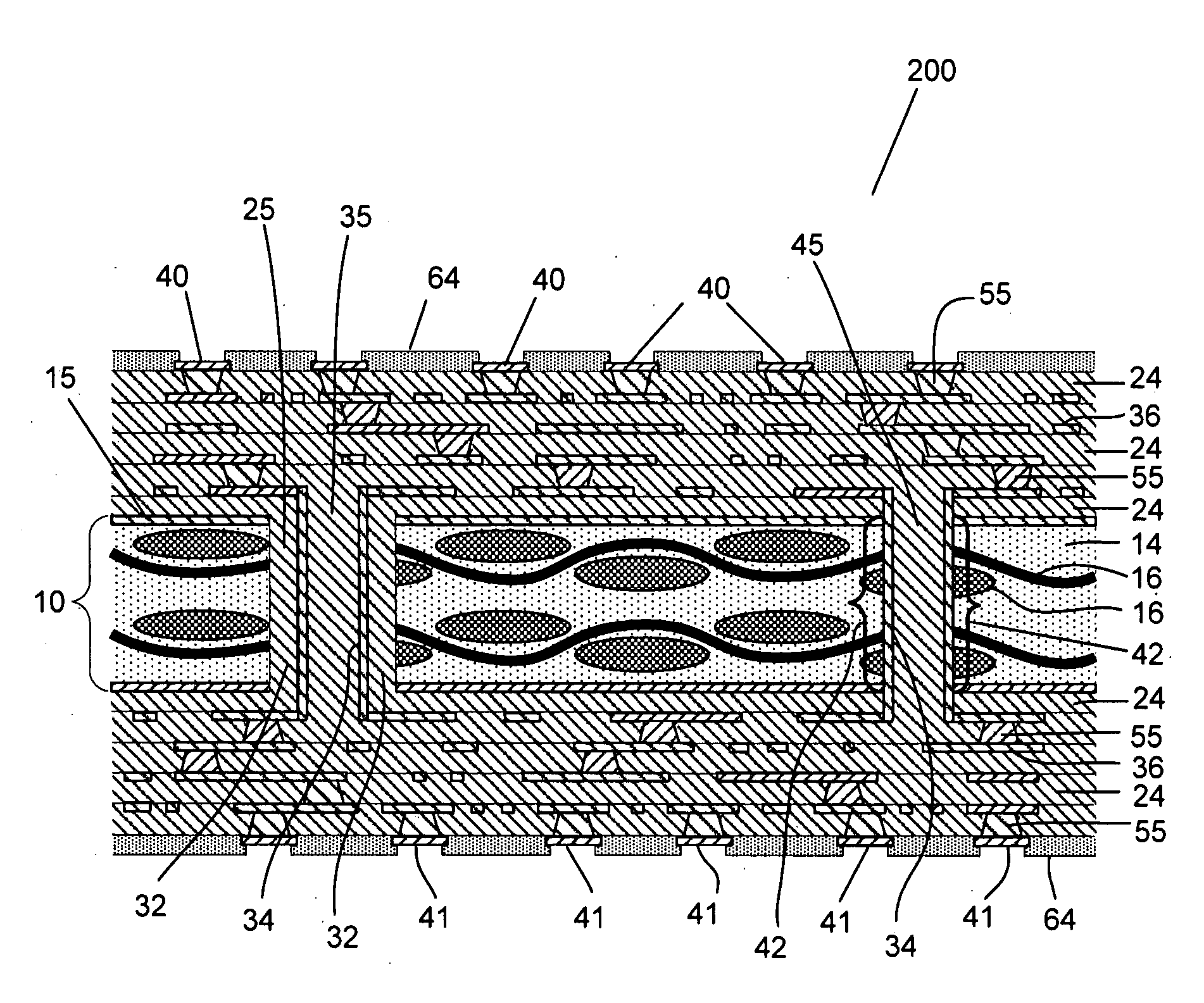
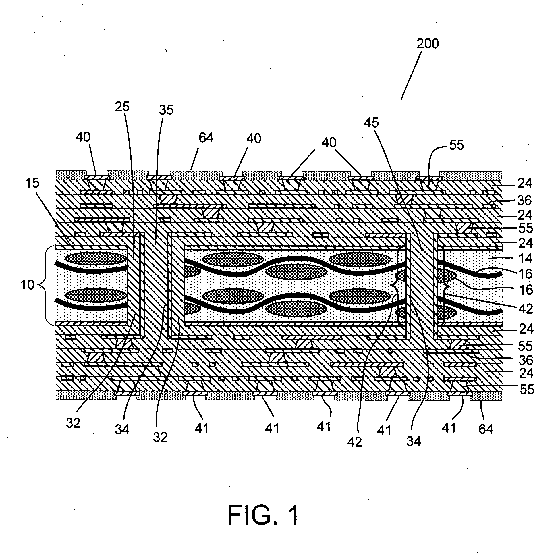
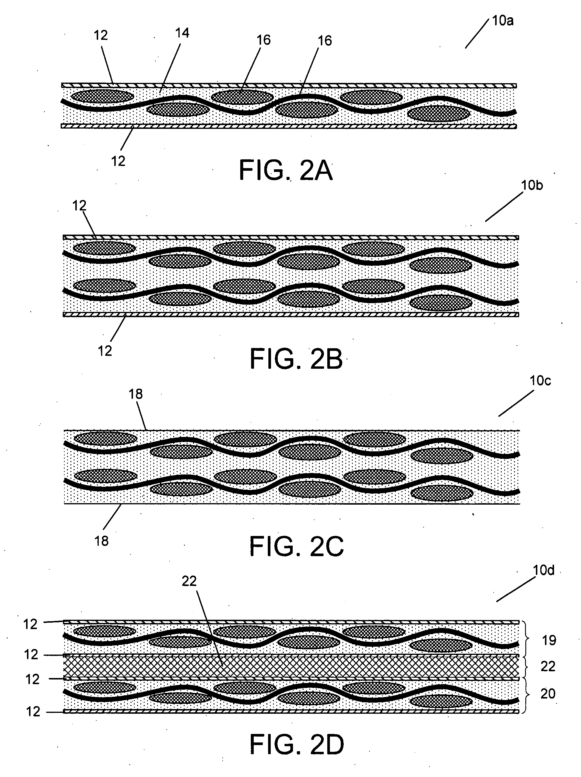
[0057] Turning now to the drawings, build-up Printed Wiring Board (PWB) substrates that include at least one core layer as an electrical layer in accordance with embodiments of the invention are shown. In addition, Integrated Circuits (ICs) that include semiconductor dies attached to PWB substrates that include at least one core layer as an electrical layer in accordance with embodiments of the invention are shown. In a number of embodiments, the core layer is constructed from a material that includes carbon. In many embodiments, the carbon material includes resin impregnated carbon fibers clad with layers of metal. In several embodiments, the layers of metal include a smooth exterior surface and a rough interior surface with protrusions that contact some of the carbon fibers. In a number of embodiments, the design of the PWB substrate is modified to improve the structural properties of the core layer compared to an unmodified PWB substrate design.

PWB Substrates

[0058] A build-up ...


PUM

PropertyMeasurementUnit
thermal conductivityaaaaaaaaaa

Abstract

Integrated circuits and processes for manufacturing integrated circuits are described that use printed wiring board substrates having a core layer that is part of the circuit of the printed wiring board. In a number of embodiments, the core layer is constructed from a carbon composite. In several embodiments, techniques are described for increasing the integrity of core layers in designs calling for high density clearance hole drilling. One embodiment of the invention includes a core layer that includes electrically conductive material and at least one build-up wiring portion formed on an outer surface of the core layer. In addition, the build-up portion comprises at least one micro wiring layer including a circuit that is electrically connected to the electrically conductive material in the core layer via a plated through hole.

Description

CROSS REFERENCE TO RELATED APPLICATION [0001] The application claims the benefit of U.S. Provisional Patent Application No. 60 / 831,108, filed Jul. 14, 2006, the contents of which are expressly incorporated herein by reference in its entirety.BACKGROUND OF THE INVENTION [0002] 1. Field of the Invention [0003] The present invention relates generally to the multilayer printed wiring boards and more specifically relates to multilayer build-up substrates that include at least one light weight constraining core that is part of the electrical circuit of the printed wiring board. [0004] 2. Description of the Related Prior Art [0005] Semiconductor device fabrication typically involves the creation of a semiconductor die using chemical processes followed by the packaging of the die. Mounting the die in the packaging includes connecting the die pad pins to the pins on the packaging. In many applications, the interconnection between the die pad pins and the pins on the packaging is achieved by ...

Claims


Application Information

Patent Timeline
Patent Type & Authority Applications(United States)
IPC IPC(8): H05K1/16
CPCH05K3/429H05K3/4608H05K3/4644H05K2201/0281H05K2201/029H01L2924/15311H05K2201/09309H05K2201/09536H05K2201/0959H01L2224/16225H05K2201/0323H01L2924/00014H01L2924/00011H01L2224/0401H05K1/0284H05K1/11H05K1/0366H05K1/0313
Inventor VASOYA, KALU K.
Owner STABLCOR TECH
Why Eureka
Try Eureka