

Multilayer capacitor array
a capacitor array and multi-layer technology, applied in the direction of fixed capacitors, stacked capacitors, fixed capacitor details, etc., can solve the problems of contradictory demands for greater capacity and greater equivalent series resistance in multi-layer capacitor arrays
- Summary
- Abstract
- Description
- Claims
- Application Information
AI Technical Summary
Benefits of technology
Problems solved by technology
Method used
Image

Examples
first embodiment
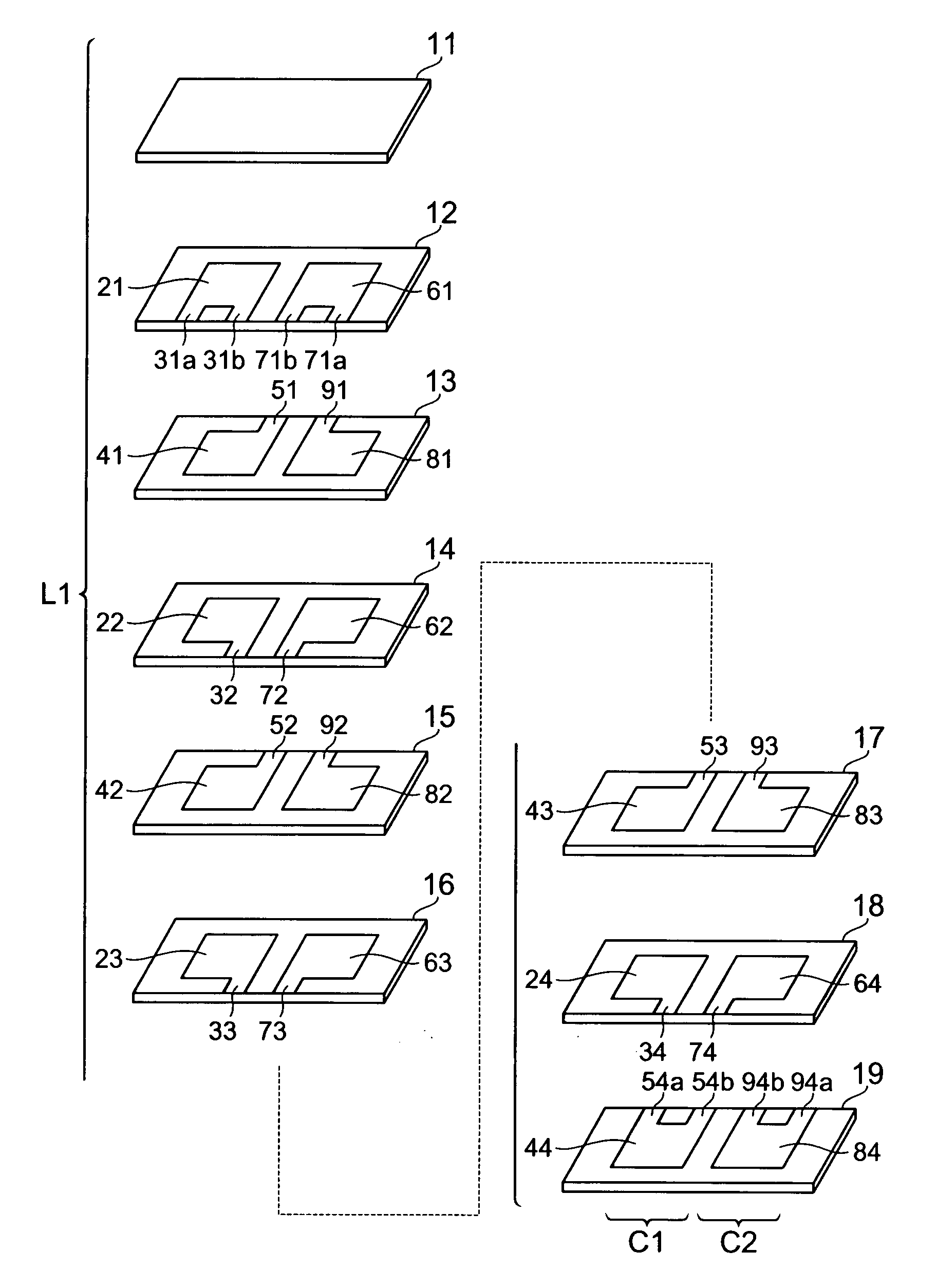
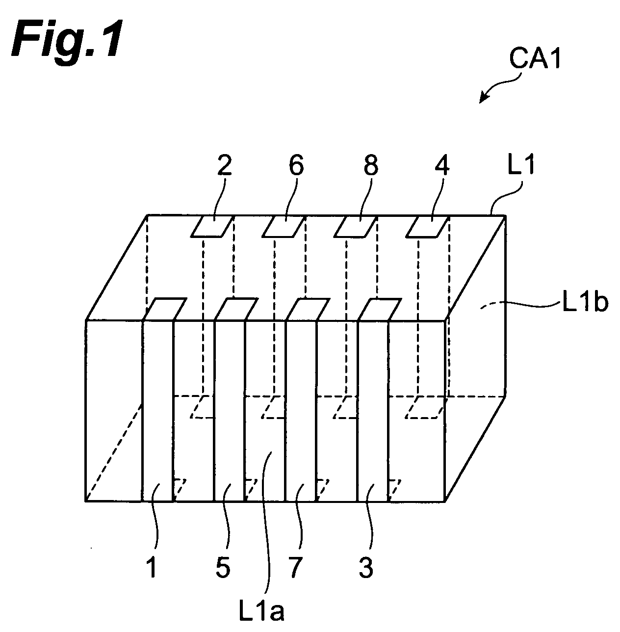
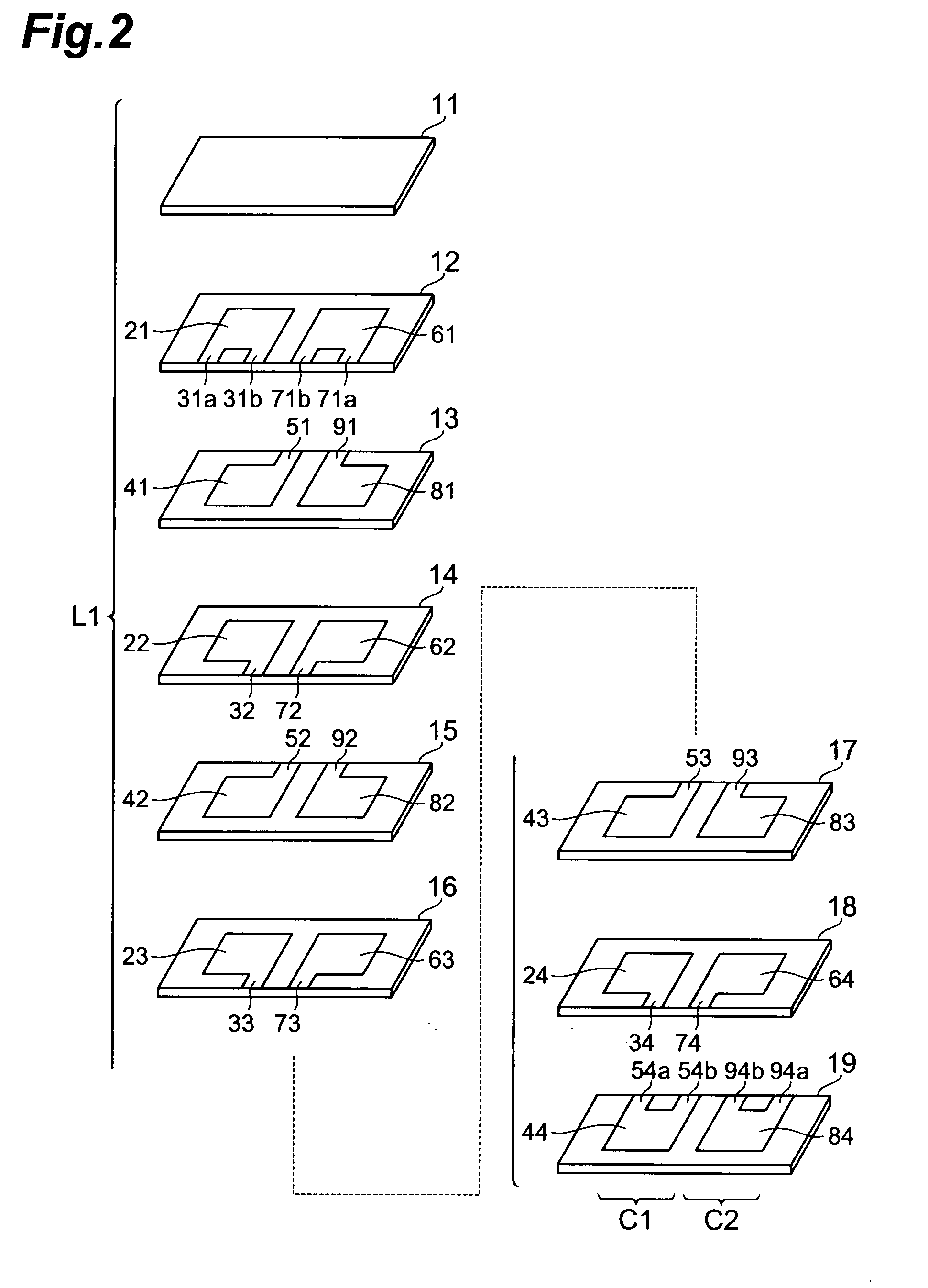
[0042]With reference to FIGS. 1 and 2, the structure of multilayer capacitor array CA1 in accordance with a first embodiment will be explained. FIG. 1 is a perspective view of the multilayer capacitor array in accordance with the first embodiment. FIG. 2 is an exploded perspective view of the multilayer body included in the multilayer capacitor array in accordance with the first embodiment.
[0043]As shown in FIG. 1, the multilayer capacitor array CA1 in accordance with the first embodiment comprises a multilayer body L1 having a substantially rectangular parallelepiped form and a plurality of outer conductors 1 to 8 formed on side faces of the multilayer body L1. The outer conductors 1 to 8 are formed, for example, by attaching and burning a conductive paste, which contains a conductive metal powder and a glass frit, onto outer surfaces of the multilayer body. A plating layer may be formed on the burned outer conductors when necessary. The plurality of outer conductors 1 to 8 are for...
second embodiment
[0077]With reference to FIGS. 3 and 4, the structure of multilayer capacitor array CA2 in accordance with a second embodiment will be explained. The multilayer capacitor array CA2 in accordance with the second embodiment differs from the multilayer capacitor array CA1 in accordance with the first embodiment in terms of the arrangement of outer conductors formed on the multilayer body. FIG. 3 is a perspective view of the multilayer capacitor array in accordance with the second embodiment. FIG. 4 is an exploded perspective view of the multilayer body included in the multilayer capacitor array in accordance with the second embodiment.
[0078]As shown in FIG. 3, the multilayer capacitor array CA2 in accordance with the second embodiment comprises a multilayer body L2 having a substantially rectangular parallelepiped form, and first to fourth terminal conductors 1 to 4 and first to fourth outer connecting conductors 5 to 8 which are a plurality of outer conductors formed on side faces of t...
third embodiment
[0098]With reference to FIGS. 5 and 6, the structure of multilayer capacitor array CA3 in accordance with a third embodiment will be explained. The multilayer capacitor array CA3 in accordance with the third embodiment differs from the multilayer capacitor array CA1 in accordance with the first embodiment in terms of the arrangement of outer conductors formed on the multilayer body. FIG. 5 is a perspective view of the multilayer capacitor array in accordance with the third embodiment. FIG. 6 is an exploded perspective view of the multilayer body included in the multilayer capacitor array in accordance with the third embodiment.
[0099]As shown in FIG. 5, the multilayer capacitor array CA3 in accordance with the third embodiment comprises a multilayer body L3 having a substantially rectangular parallelepiped form, and first to fourth terminal conductors 1 to 4 and first to fourth outer connecting conductors 5 to 8 which are a plurality of outer conductors formed on side faces of the mu...
PUM
 Abstract
Description
Claims
Application Information