
Semiconductor device and method of manufacturing the same

a semiconductor device and semiconductor technology, applied in semiconductor devices, diodes, electrical devices, etc., can solve the problems of reducing the reliability of a semiconductor device, high occlusion position of a cavity, etc., to prevent the occlusion position of the cavity from being located, the effect of wide width and easy operation

Inactive Publication Date: 2008-01-17
RENESAS ELECTRONICS CORP
View PDF3 Cites 19 Cited by
  • Summary
  • Abstract
  • Description
  • Claims
  • Application Information

AI Technical Summary

Benefits of technology

The present invention provides a semiconductor device and a manufacturing method that can reliably have a cavity between adjacent convex patterns without causing corrosion or a decrease in reliability of the semiconductor device. The semiconductor device includes a first insulating film that covers the side surfaces of the convex patterns and a second insulating film that covers the upper surface and side surface of the first insulating film. The second insulating film is formed using film formation conditions that are easier to do horizontal direction growth than the first insulating film. This prevents the cleaning liquid from corrobing the cavity and ensures reliable flattening of the semiconductor device. The manufacturing method includes steps of forming the convex patterns, forming the first insulating film, and forming the second insulating film. The position of the cavity is higher than the upper surface of the control gate, which prevents corrosion during chemical mechanical polishing.

Problems solved by technology

According to the technology of above-mentioned Patent Reference 2, there was a problem that a cavity would not be formed between wirings when the insulating film which covers a wiring is formed by a method with sufficient step coverage nature (step coverage).
Although a cavity will be formed between wirings on the other hand when the insulating film which covers a wiring is formed by the method that step coverage nature is bad, the upper occlusion position of a cavity becomes high.
In this case, since the cleaning liquid used by the CMP method sinks in a cavity and the wiring material was made to corrode, there was a problem that the reliability of a semiconductor device fell.

Method used


Image

  • Semiconductor device and method of manufacturing the same
  • Semiconductor device and method of manufacturing the same
  • Semiconductor device and method of manufacturing the same

Examples


embodiment 1

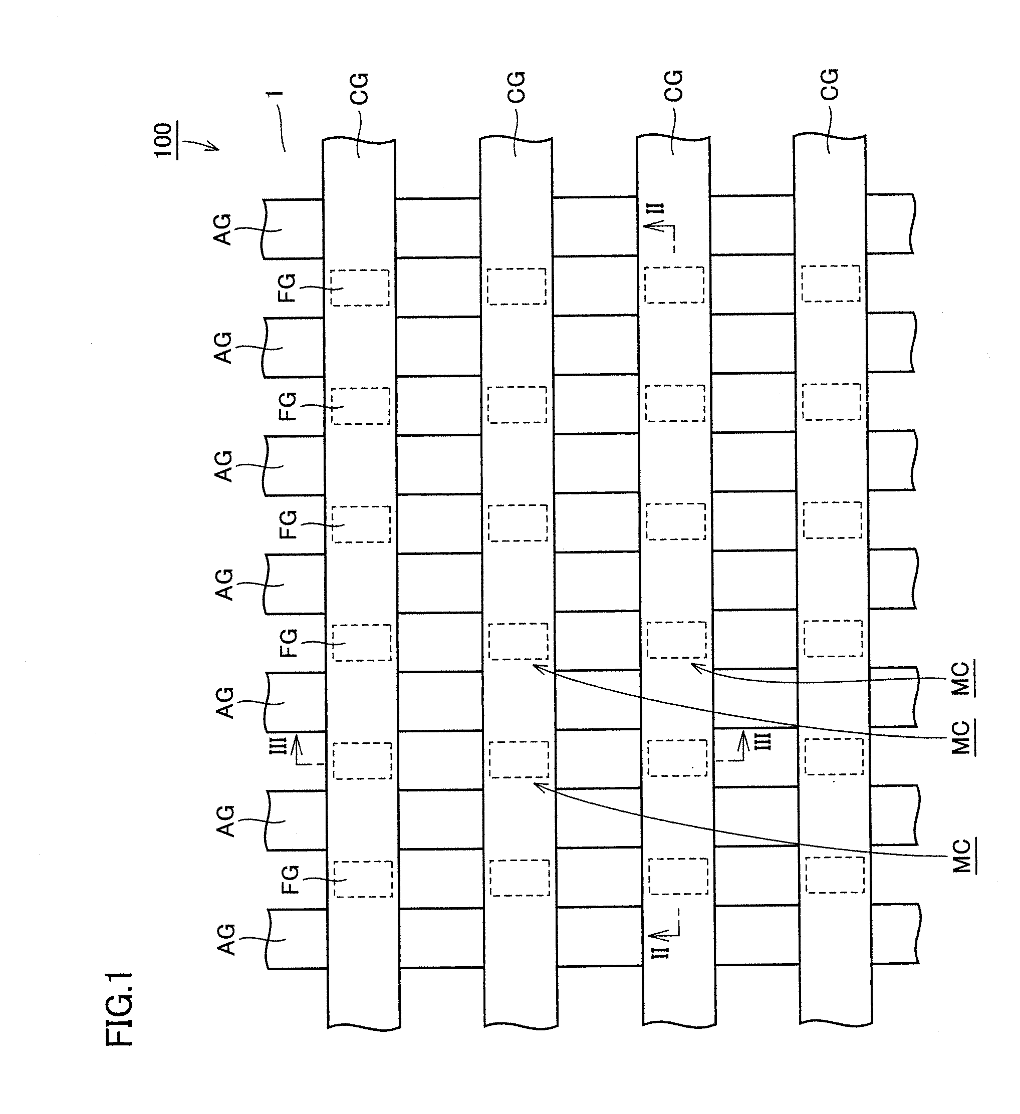
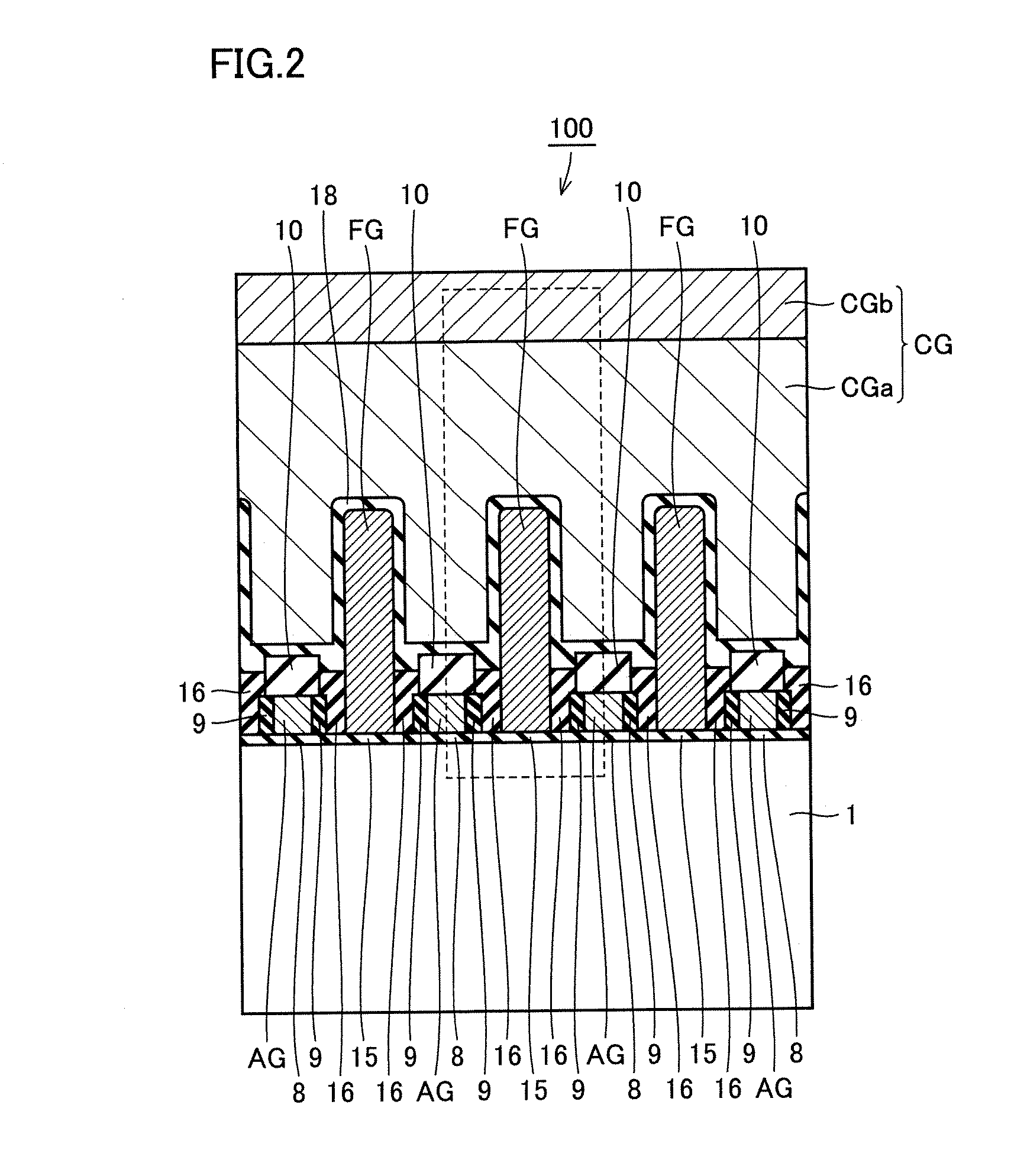
[0043]Embodiment 1 of the present invention is one embodiment when the present invention is applied to the nonvolatile semiconductor memory which has Assist Gate. First, FIG. 1-FIG. 3 are used and explained about the structure.

[0044]FIG. 1 is a plan view showing roughly the structure of the semiconductor device in Embodiment 1 of the present invention. Each of FIG. 2 and FIG. 3 is an outline cross-sectional view which goes along the II-II line and III-III line of FIG. 1.

[0045]With reference to FIG. 1, semiconductor device 100 has a memory cell array by which a plurality of memory cell MC has been arranged at matrix form. In this memory cell array, each of a plurality of Assist Gate AG formed on the front surface of semiconductor substrate 1 is arranged so that it may run in parallel mutually to the longitudinal direction in a drawing. In the direction (horizontal direction in a drawing) which intersects perpendicularly with these Assist Gate AG, each of a plurality of control gate C...

embodiment 2

[0095]Embodiment 2 of the present invention is one embodiment when the present invention is applied to the nonvolatile semiconductor memory which has Assist Gate. In the manufacturing method of this embodiment, the sputtering redeposition step of first insulating film 11 is performed between the film formation step of first insulating film 11, and the film formation step of second insulating film 12. Below, FIG. 4-FIG. 6, and FIG. 9-FIG. 11 are used and explained about this embodiment.

[0096]FIGS. 9A and 9B are outline cross-sectional views showing the state before sputtering redeposition processing FIG. 9A and the state after sputtering redeposition processing FIG. 9B in Embodiment 2 of the present invention, and is a cross-sectional view of the region corresponding to the region surrounded in the dashed line part of FIG. 6. FIG. 10 and FIG. 11 are the outline cross-sectional views showing the manufacturing method of the semiconductor device in Embodiment 2 of the present invention ...

embodiment 3

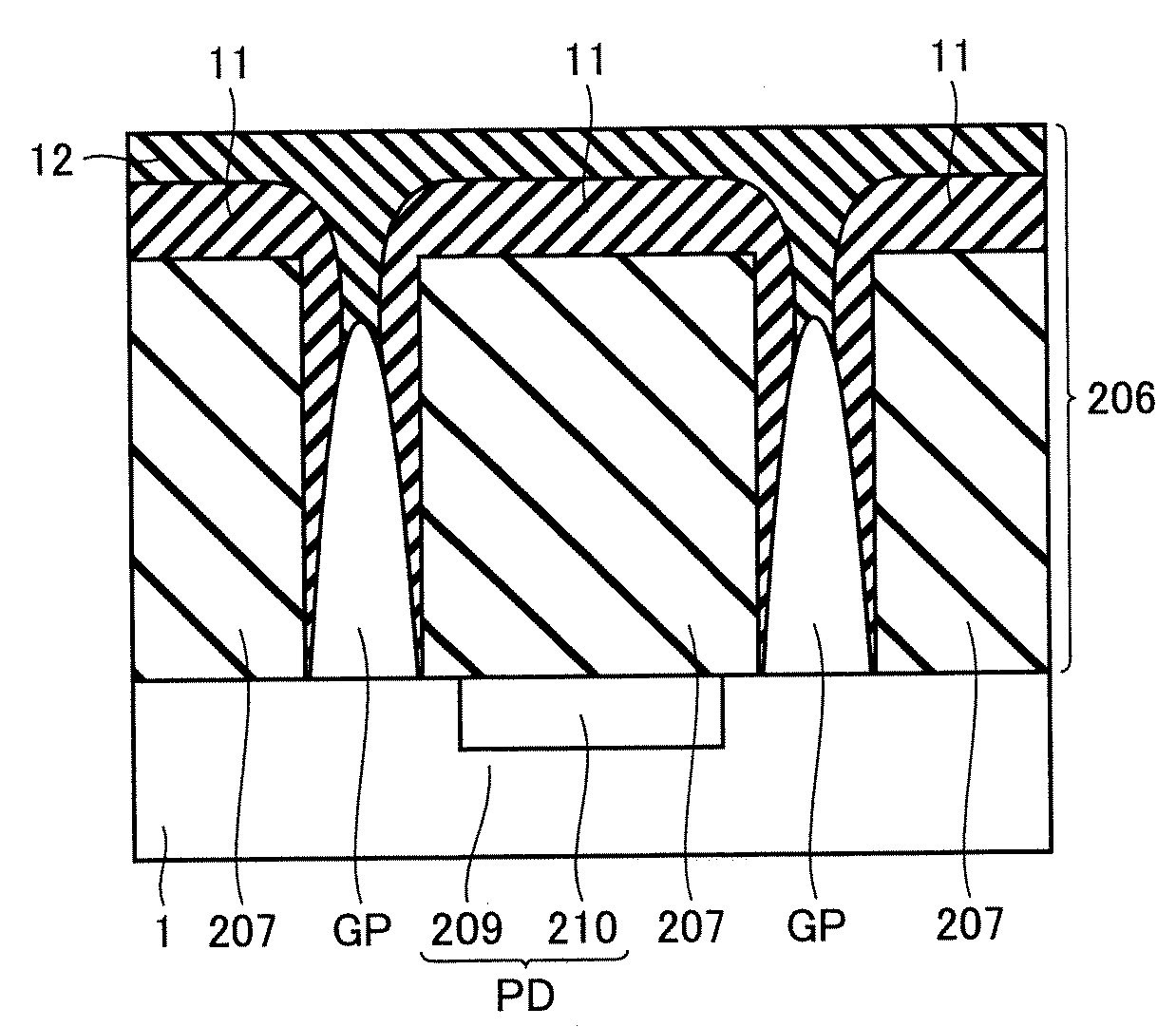
[0111]Embodiment 3 of the present invention is one embodiment when the present invention is applied to the semiconductor device provided with the image sensor. First, FIG. 12 and FIG. 13 are used and explained about the structure.

[0112]FIG. 12 is a cross-sectional view showing roughly the structure of the semiconductor device provided with the image sensor in this embodiment. With reference to FIG. 12, semiconductor device 200 provided with the image sensor is provided with photo diode PD as an image sensor formed in semiconductor substrate 1. This photo diode PD is formed by n type impurity region 210 and p type well region 209.

[0113]First interlayer insulating layer 206 is formed in the front surface of semiconductor substrate 1. The detail of the structure of first interlayer insulating layer 206 is mentioned later. The upper surface of first interlayer insulating layer 206 is CMP polished surface 208 polished by CMP. Patterned wiring layer 204 and second interlayer insulating la...


PUM


Abstract

When microfabrication is done, a reliable semiconductor device is offered.A semiconductor device has a semiconductor substrate which has a main front surface, a plurality of convex patterns formed on the main front surface of a semiconductor substrate so that each might have a floating gate and a control gate, a first insulating film formed so that the upper surface and the side surface of each of a plurality of convex patterns might be covered, and so that width might become large rather than the portion which covers the lower part side surface of a convex pattern in the portion which covers an upper part side surface, and a second insulating film that covers the upper surface and the side surface of the first insulating film so that the cavity between the adjacent convex patterns may be occluded. The position occluded by the second insulating film of a cavity is a position higher than the upper surface of a floating gate, and is a position lower than the upper surface of a control gate.

Description

CROSS-REFERENCE TO RELATED APPLICATION[0001]The present application claims priority from Japanese patent application No. 2006-191358 filed on Jul. 12, 2006, the content of which is hereby incorporated by reference into this application.FIELD OF THE INVENTION[0002]The present invention relates to a semiconductor device and its manufacturing method, and particularly relates to the semiconductor device which has a cavity part, and its manufacturing method.DESCRIPTION OF THE BACKGROUND ART[0003]A miniaturization and microfabrication of the semiconductor device are advanced from the former, and how to make it small without causing various trouble has been an important problem.[0004]And in recent years, in order to solve the above-mentioned problem, the AG-AND (Assist Gate-AND) type flash memory provided with a plurality of Assist Gate's for forming an inversion layer in the main front surface side of a semiconductor substrate, a floating gate formed between these Assist Gate's, and a con...

Claims


Application Information

Patent Timeline
Patent Type & Authority Applications(United States)
IPC IPC(8): H01L21/469H01L29/788
CPCH01L21/28273H01L21/7682H01L21/76834H01L27/115H01L29/42324H01L27/14627H01L27/14632H01L27/14643H01L27/14689H01L27/11521H01L29/40114H10B69/00H10B41/30
Inventor MURATA, TATSUNORIASAI, KOYUIUCHI, HIROAKI
Owner RENESAS ELECTRONICS CORP
Learn More