Substrate processing apparatus and substrate processing method

Inactive Publication Date: 2008-01-24
SCREEN HLDG CO LTD
View PDF5 Cites 25 Cited by
  • Summary
  • Abstract
  • Description
  • Claims
  • Application Information

AI Technical Summary

Benefits of technology

[0012]However, since IPA vapor supplied onto the wafer quickly leaves the wafer owing to an air flow which develops by the rotation of the wafer according to the IPA vapor supplying method de

Problems solved by technology

However, since IPA vapor supplied onto the wafer quickly leaves the wafer owing to an air flow which develops by the rotation of the wafer according to the IPA vapor supplying method described in JP-A-2003-197590, it is not easy to dissolve IPA in deionized water which adheres to the wafer and it is not possible to fully enjoy the effect of prevention of pattern destruction.
Meanwhile, although the air flow which develops by the rotation of the wafer is prevented from pushing away IPA vapor from above the wafer since the dry guide covers the top or bottom surface of the wa

Method used


Image

  • Substrate processing apparatus and substrate processing method
  • Substrate processing apparatus and substrate processing method
  • Substrate processing apparatus and substrate processing method

Examples


Example

[0027]A first embodiment of the invention will now be described in detail with reference to the associated drawings.

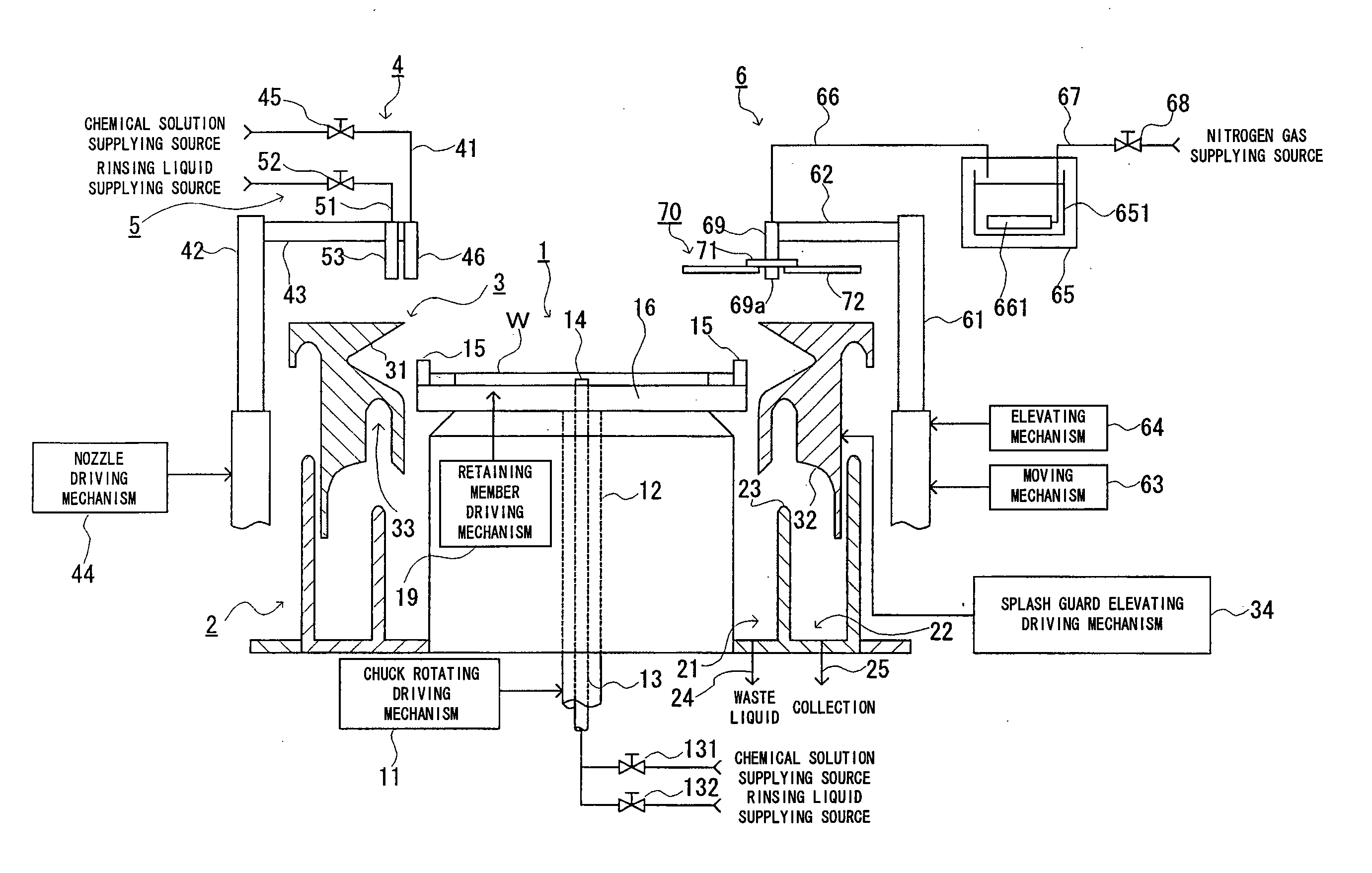
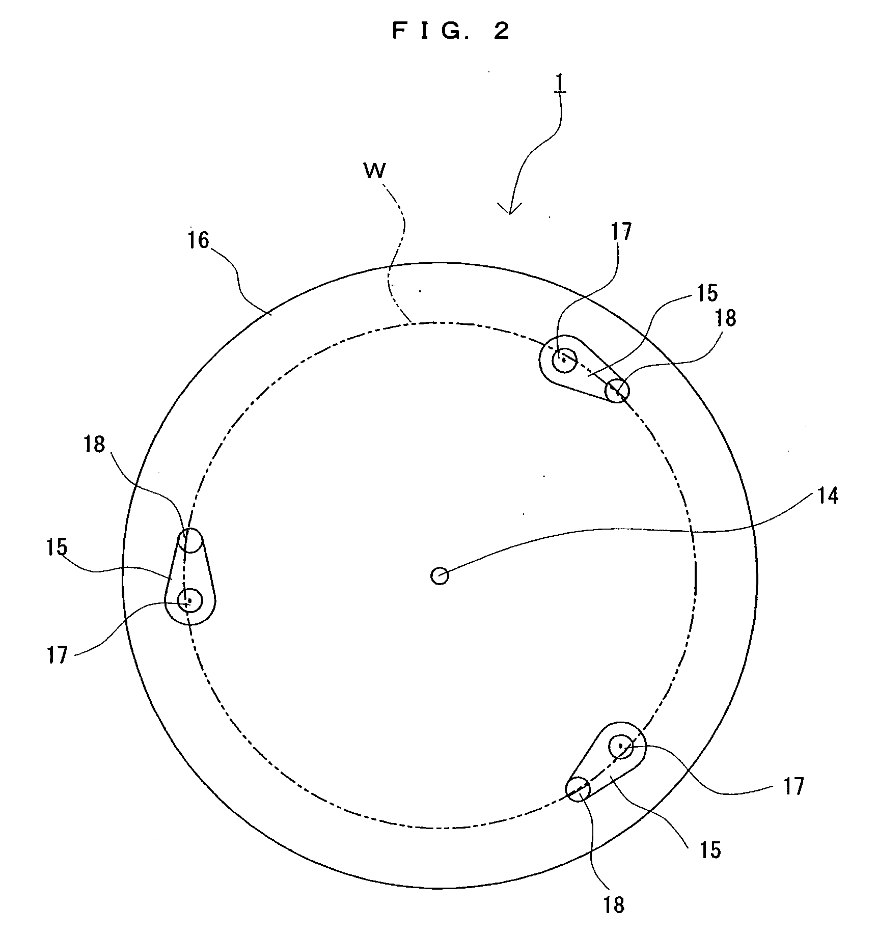
[0028]FIG. 1 is a schematic cross sectional view which shows a structure of a substrate processing apparatus according to the first embodiment of the invention. This substrate processing apparatus is a cleaning and drying apparatus which cleans semiconductor wafers (hereinafter referred to as “wafers”) W serving as substrates one by one and dries thus cleaned wafers W. This substrate processing apparatus comprises a spin chuck 1, a processing cup 2 which houses the spin chuck 1, a splash guard 3 which is disposed in relation to the processing cup 2, a chemical solution supplying mechanism 4, a chemical solution and a rinsing liquid supplying mechanism 5, and an organic solvent component supplying mechanism 6. The spin chuck 1 holds the wafer W approximately horizontally and rotates the wafer W about the axis line of rotation which penetrates the center of the wafer app...

Example

[0064]Next, a second embodiment of the present invention will be described.

[0065]FIG. 6 is a schematic side view for describing the structure of a substrate processing apparatus according to the second embodiment of the invention, and FIG. 7 is a schematic top plan view showing the vicinity of the organic solvent component nozzle. A section around the organic solvent component nozzle is shown in FIG. 6, and portions corresponding to FIG. 1 described earlier are denoted at the same reference symbols.

[0066]In the second embodiment, the substrate processing apparatus comprises a rinsing liquid supplying mechanism 8 for supplying a rinsing liquid to the wafer W on the downstream side relative to the organic solvent component nozzle 69 in the scanning direction (which is the direction denoted at the arrow Q in FIG. 7). The rinsing liquid supplying mechanism 8 comprises a rinse nozzle 83, a rinsing liquid supplying pipe 81, and a valve 82. The rinse nozzle 83 is disposed, in the tip end o...

Example

[0074]Further, in the first and the second embodiments described above, although the arm 62 moves at the constant speed when the organic solvent component nozzle 69 moves at Step S5, the arm 62 may move at a varying speed while traveling from the central position of the wafer W toward the periphery of the wafer W. To be more specific, the control device 7 may control the moving mechanism 63 so that the organic solvent component nozzle 69 move faster in the vicinity of the central position of the wafer W than in the vicinity of the periphery of the wafer W. According to this modification, it is possible to maintain a uniform amount of the organic solvent component which is dissolved in the liquid film of the rinsing liquid per unit area all over the surface of the wafer W, and hence, to evenly dry the entire wafer W while sufficiently preventing pattern destruction.

[0075]In addition, in the first and the second embodiments described above, the organic solvent component nozzle 69 is d...


PUM


Abstract

Above a wafer which is held by a spin chuck, a blocking member whose opposed surface to the wafer is approximately horizontal is disposed at a higher position than an organic solvent component supplying outlet which is able to move from a central position of the wafer toward the periphery of the wafer. An organic solvent component nozzle scans (moves) together with the blocking member, thereby efficiently supplying a gas containing an organic solvent component discharged from the organic solvent component supplying outlet onto a surface of the wafer without getting discharged from the vicinity of the surface of the wafer owing to the blocking member. Hence, when the organic solvent component nozzle scans (moves), the concentration of the organic solvent component is always high near the organic solvent component supplying outlet.

Description

CROSS REFERENCE TO RELATED APPLICATION[0001]The disclosure of Japanese Patent Application No. 2006-195026 filed Jul. 18, 2006 including specification, drawings and claims is incorporated herein by reference in its entirety.BACKGROUND OF THE INVENTION[0002]1. Field of the Invention[0003]The present invention relates to a substrate processing apparatus for and a substrate processing method of drying a substrate to which a liquid adheres. The present invention particularly relates to a substrate processing apparatus and a substrate processing method which, in a single wafer processing, dry a substrate after rinsing processing is performed. Substrates to be dried include, for example, semiconductor wafers, substrates for liquid crystal display, substrates for plasma display, substrates for FED (Field Emission Display), substrates for optical disks, substrates for magnetic disks, substrates for magnet-optical disks, substrates for photomask, etc.[0004]2. Description of the Related Art[00...

Claims


Application Information

Patent Timeline
IPC IPC(8): B08B3/08B08B5/04
CPCH01L21/67051H01L21/68728H01L21/6708
Inventor MIYA, KATSUHIKOIZUMI, AKIRA
Owner SCREEN HLDG CO LTD
Why Eureka
Try Eureka