Light Emitting Element With A Plurality Of Cells Bonded, Method Of Manufacturing The Same, And Light Emitting Device Using The Same

a technology cells, which is applied in the direction of solid-state devices, electric lighting sources, electric light sources, etc., can solve the problems of affecting the production efficiency of light emitting elements, so as to simplify the manufacturing process of light emitting devices and reduce the fraction of defectives. , the effect of high voltag

Active Publication Date: 2008-01-24
SEOUL VIOSYS CO LTD
View PDF6 Cites 44 Cited by
  • Summary
  • Abstract
  • Description
  • Claims
  • Application Information

AI Technical Summary

Benefits of technology

[0014] According to the present invention, it is possible to manufacture a light emitting device capable of being used for illumination through a single light emitting element with a plurality of light emitting cells connected in series.
[0015] Further, since a plurality of light emitting cells are electrically connected at a wafer level, it is possible to manufacture a light emitting element capable of emitting light with a high voltage and a household AC power source.
[0016] Furthermore, since a light emitting element with a plurality of light emitting cells electrically connected on a substrate is used, it is possible to simplify a manufacturing process of a light emitting device for illumination, to decrease a fraction defective occurring in manufacturing a light
[0017] emitting device for illumination, and to mass-produce the light emitting device for illumination.
[0018] In addition, electrodes of a light emitting element chip and a predetermined rectifying circuit are connected to minimize a ripple factor in AC driving, thereby maximizing light emitting efficiency and to control a load on an LED array through connection of a resistor, thereby protecting the light emitting element chip.

Problems solved by technology

However, if a light emitting device for general illumination having the aforementioned structure is manufactured according to the prior art, there is a problem in that the metal wiring process should be performed for a large number of elements one by one so that processing steps increase in number and are complicated.
As the number of the process steps increases, a fraction defective also increases, thereby impeding mass production.
Further, there may be a case where metal wiring becomes a short circuit due to a certain shock so that the operations of light emitting elements are stopped.
Furthermore, there is a disadvantage in that spaces occupied due to serial array of respective light emitting elements are expanded so that the size of a lamp considerably becomes large.
However, different electric signals should be applied in respective vertical and horizontal directions and the electric signals should be supplied in an address manner so as to cause the elements arranged in the matrix form to emit light, which is very difficult to control.
Further, wiring may be disconnected due to the array in the form of a matrix, and a great deal of interference occurs in wire-overlapping areas.
Furthermore, there is a problem in that the aforementioned matrix-shaped structure is not applicable to a light emitting device for illumination to which a high voltage is applied.

Method used


Image

  • Light Emitting Element With A Plurality Of Cells Bonded, Method Of Manufacturing The Same, And Light Emitting Device Using The Same
  • Light Emitting Element With A Plurality Of Cells Bonded, Method Of Manufacturing The Same, And Light Emitting Device Using The Same
  • Light Emitting Element With A Plurality Of Cells Bonded, Method Of Manufacturing The Same, And Light Emitting Device Using The Same

Examples


first embodiment

[0090]FIG. 8 is a conceptual diagram illustrating a light emitting element according to the present invention.

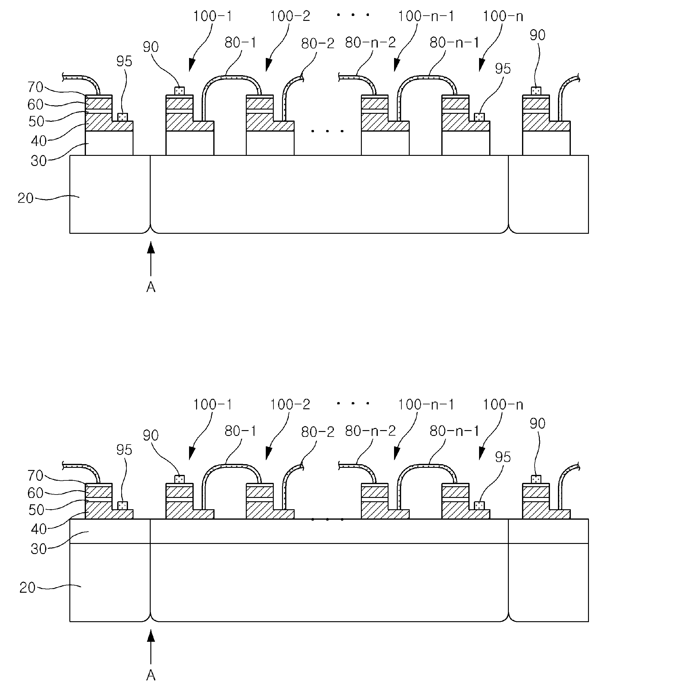
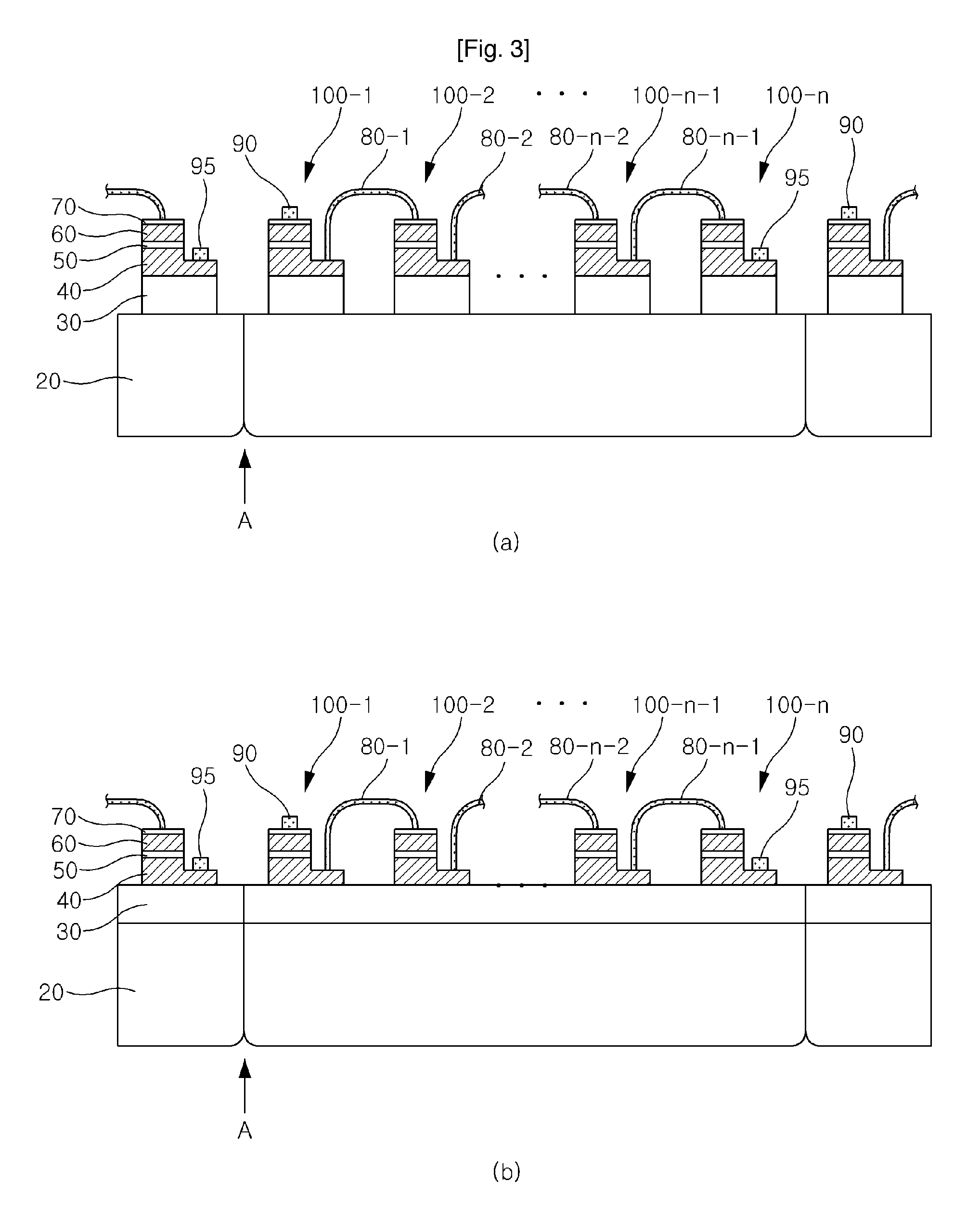
[0091] Referring to FIG. 8, in the light emitting element 300 of this embodiment, a plurality of light emitting cells 100 and 200 connected in series are electrically connected to the outside.

[0092] In the light emitting element 300, first and second electrodes 310 and 320 are formed on an N-type pad 95 or 210 and a P-type pad 90 or 250 through a wiring process, respectively. The first and the second electrodes 310 and 320 refer to an anode electrode and a cathode electrode, respectively. Accordingly, a single light emitting element 300 with the plurality of light emitting cells 100 and 200 connected in series is manufactured.

[0093] In addition, it is possible to provide a light emitting element with an additional controller added thereto so that the light emitting element can be operated even in AC driving.

[0094] This embodiment is not limited to the case where a plurali...

third embodiment

[0100]FIG. 10 is a conceptual diagram illustrating a light emitting element according to the present invention.

[0101] Referring to FIG. 10, the light emitting element 300 of this embodiment comprises a plurality of light emitting cells 100 and 200 connected in series, a rectifying bridge unit 301 for applying a predetermined current to the light emitting cells 100 and 200, and electrodes 310 and 320 connected to the rectifying bridge unit 301.

[0102] In this embodiment, the plurality of light emitting cells 100 and 200 are electrically connected to an external power source not directly but through the rectifying bridge unit 301 connected to first and second electrodes 310 and 320. The rectifying bridge unit 301 comprises a first diode D1 connected to the first electrode 310 and an anode terminal of the light emitting cells 100 and 200, a second diode D2 connected to the second electrode 320 and an anode terminal of the light emitting cells 100 and 200, a third diode D3 connected to ...

fourth embodiment

[0104]FIG. 11 is a conceptual diagram illustrating a light emitting element according to the present invention.

[0105] Referring to FIG. 11, the light emitting element 300 of this embodiment comprises a plurality of light emitting cells 100 and 200 connected in series, a rectifying bridge unit 301 for applying a predetermined current to the light emitting cells 100 and 200, and electrodes 310 to 340 connected to the light emitting cells 100 and 200 and the rectifying bridge unit 301.

[0106] In this embodiment, the plurality of serially connected light emitting cells 100 and 200 are electrically connected to an external power source through second and fourth electrodes 320 and 340, and through the rectifying bridge unit 301 connected to first and third electrodes 310 and 330. The same power source or different power sources may be connected to the light emitting cells 100 and 200 and the rectifying bridge unit 301.

[0107] The rectifying bridge unit 301 comprises a first diode D1 conne...


PUM


Abstract

The present invention relates to a light emitting element with arrayed cells, a method of manufacturing the same, and a light emitting device using the same. The present invention provides a light emitting element including a light emitting cell block with a plurality of light emitting cells connected in series or parallel on a single substrate, and a method of manufacturing the same, wherein each of the plurality of light emitting cells includes an N-type semiconductor layer and a P-type semiconductor layer, and the N-type semiconductor layer of one light emitting cell is electrically connected to the P-type semiconductor layer of another adjacent light emitting cell. Further, the present invention provides a light emitting device including a light emitting element with a plurality of light emitting cells connected in series. Accordingly, it is possible to simplify a manufacturing process of a light emitting device for illumination capable of being used with a household AC power source, to decrease a fraction defective occurring in manufacturing a light emitting device for illumination, and to mass-produce the light emitting device for illumination. Further, there is an advantage in that DC driving efficiency can be enhanced in an AC operation by installing a predetermined rectifying circuit outside the light emitting element.

Description

TECHNICAL FIELD [0001] The present invention relates to a light emitting element with a plurality of cells bonded, a method of manufacturing the same, and a light emitting device using the same. More particularly, the present invention relates to a single light emitting element with a plurality of light emitting cells arrayed on a single substrate, a method of manufacturing the same, and a light emitting device using the same. BACKGROUND ART [0002] A light emitting diode refers to an element in which minority carriers (electrons or holes) injected using a p-n junction structure of a semiconductor are produced and certain light is emitted through recombination thereof. Such light emitting diodes have been used as display devices and backlights, and studies on application of the light emitting diodes to general illumination have been actively conducted. [0003] This is because light emitting diodes have less electric power consumption and longer lifespan as compared with existing bulbs...

Claims


Application Information

Patent Timeline
Patent Type & Authority Applications(United States)
IPC IPC(8): H01L33/00H01L21/00H01L33/08H01L33/12H01L33/32H01L33/44H05B44/00
CPCH01L25/0753H01L33/62H05B33/0803H05B33/0809H05B33/0821H01L33/08H01L2224/48137H01L2224/48091H01L2224/49107H01L2924/00014H01L2924/00H05B45/40H05B45/36H05B45/42
Inventor LEE, CHUNG-HOONLEE, KEON-YOUNGYVES, LACROIX
Owner SEOUL VIOSYS CO LTD
Why Eureka
Try Eureka