

Flip-chip semiconductor package and chip carrier thereof
- Summary
- Abstract
- Description
- Claims
- Application Information
AI Technical Summary
Benefits of technology
Problems solved by technology
Method used
Image

Examples
Embodiment Construction
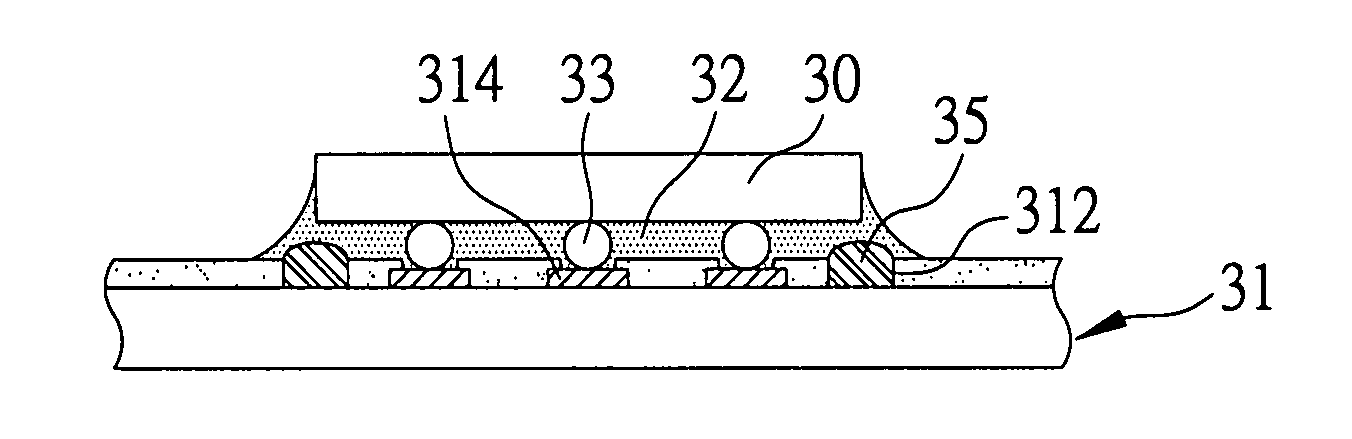
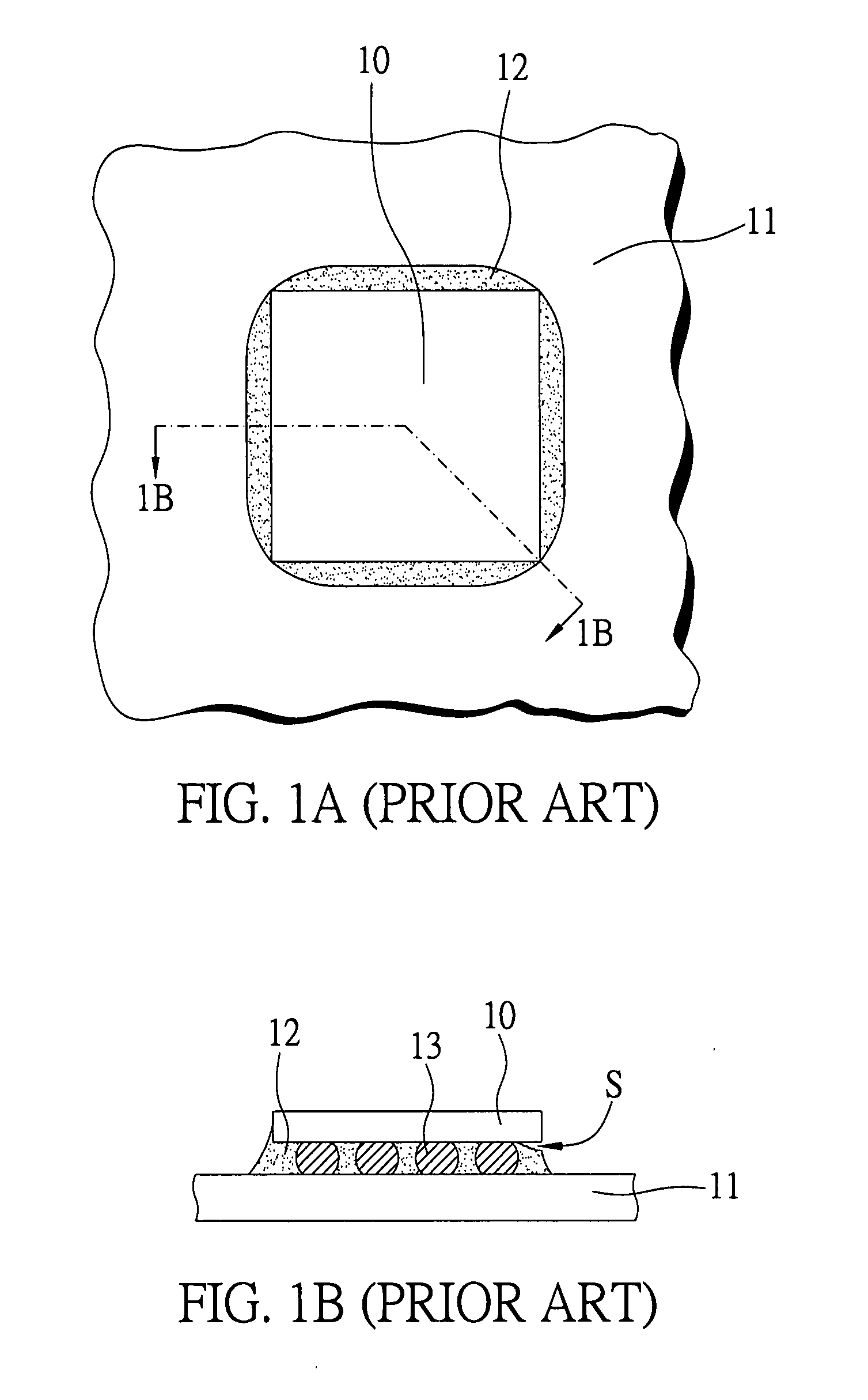
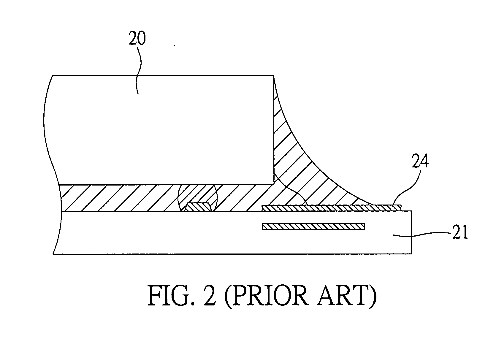
[0025] In the following description, numerous specific details are given to provide a thorough understanding of the invention. However, it will be apparent that the invention may be practiced without these specific details. In order to avoid obscuring the present invention, some well-known configurations and process steps are not disclosed in detail.
[0026] Likewise, the drawings showing embodiments of the structure are semi-diagrammatic and not to scale and, particularly, some of the dimensions are for the clarity of presentation and are shown greatly exaggerated in the drawing. Similarly, although the views in the drawings for ease of description generally show similar orientations, this depiction in the drawings is arbitrary for the most part. Generally, the invention can be operated in any orientation.
[0027] For expository purposes, the term “horizontal” as used herein is defined as a plane parallel to the plane or surface of the substrate, regardless of its orientation. The te...
PUM
 Abstract
Description
Claims
Application Information