

Fabrication method of semiconductor device
a technology of semiconductor devices and fabrication methods, applied in the direction of semiconductor devices, basic electric elements, electrical equipment, etc., can solve the problems of deteriorating manufacturing efficiency, taking time for switching work and subsequent adjustment work,
- Summary
- Abstract
- Description
- Claims
- Application Information
AI Technical Summary
Benefits of technology
Problems solved by technology
Method used
Image

Examples
first embodiment
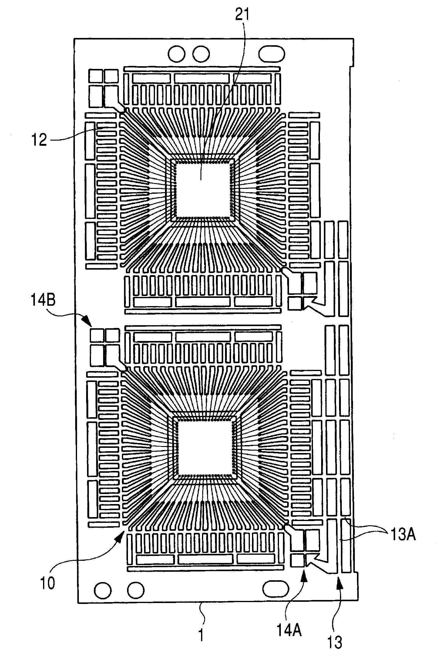
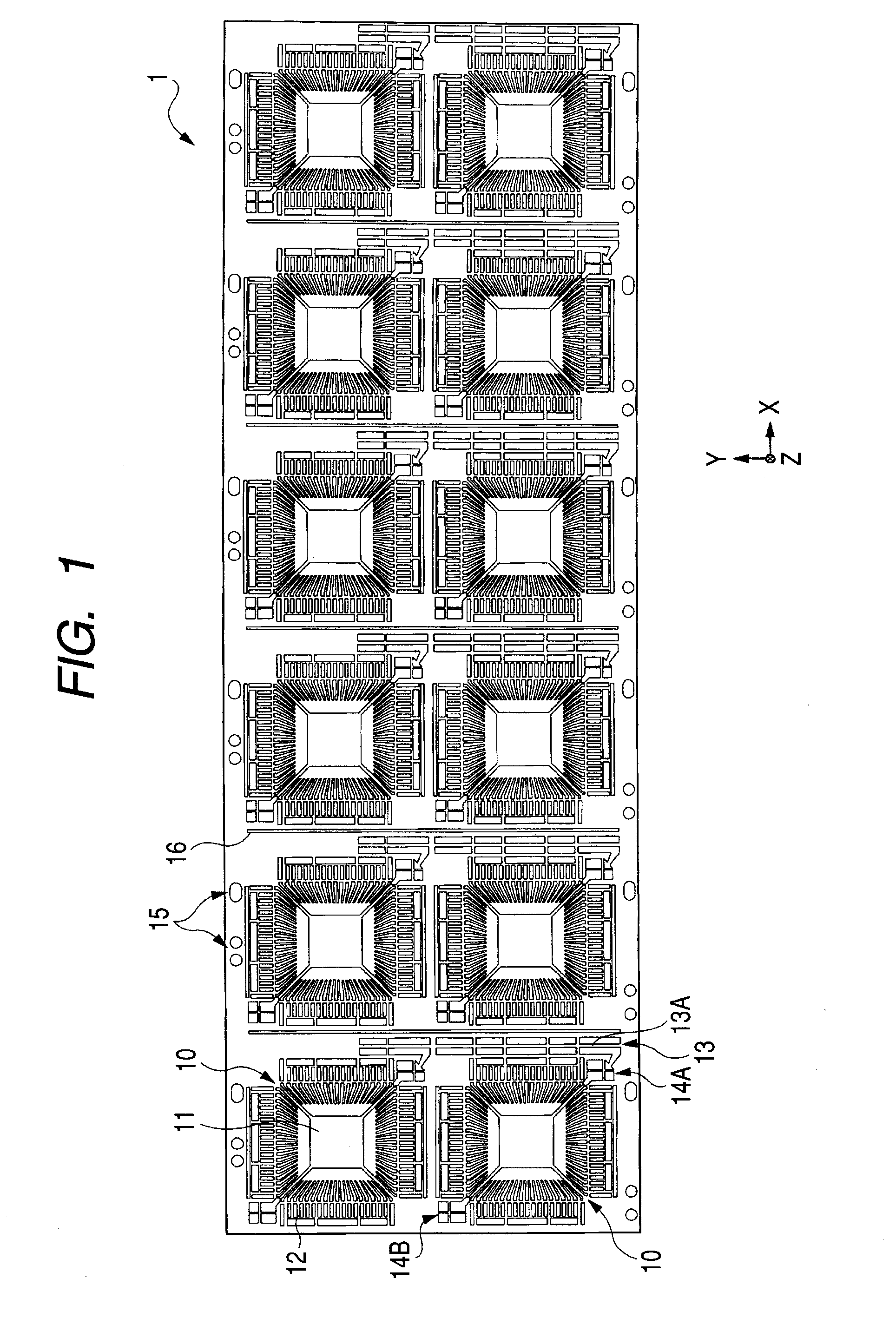
[0085]FIG. 1 is a plan view showing an example of outline of a lead frame (base) 1 used in this first embodiment. The lead frame 1 shown in FIG. 1 is, for example, a matrix type lead frame for QFP (Quad Flat Package). According to the structure of this lead frame, if it is assumed that the longitudinal direction (X-axis direction) of the lead frame 1 is column and the direction (Y-axis direction) orthogonal to the column direction is row, unit frames 10 each corresponding to one product are arranged in 6 rows by 2 columns. The matrix type lead frame used in this first embodiment has two or more unit frames in each of row and column. Further, in this first embodiment, the thickness direction of the lead frame orthogonal to the above X and Y axes is assumed to be Z-axis direction.
[0086]Each unit frame 10 includes a tab 11, a large number of leads 12 arranged so as to surround the tab 11, a gate portion 14A formed at a corner of a package area (cavity portion) as a resin sealing area i...
second embodiment
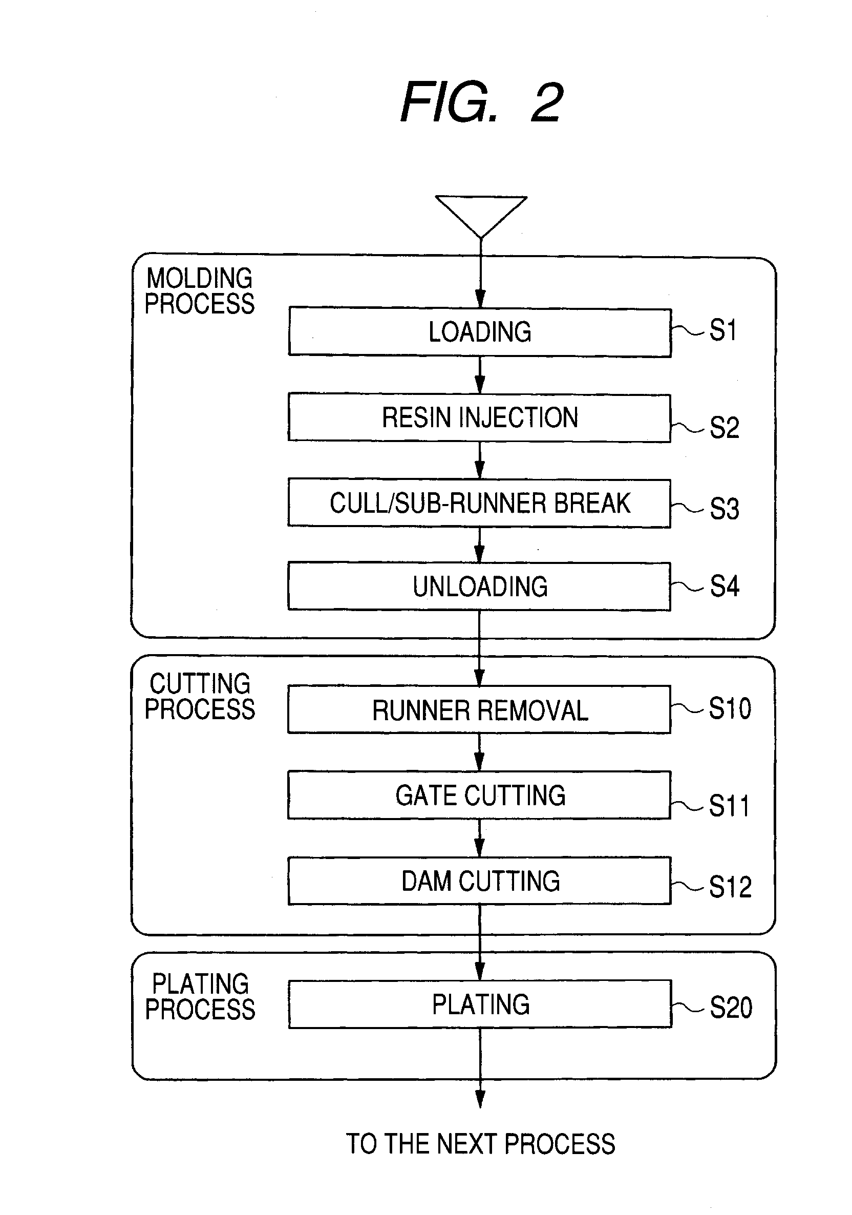
[0142]This second embodiment concerns a case where the width (see FIG. 1) in Y direction of the lead frame 1 is narrow. The following description is provided about the operation of the molding press sets MPS1 to MPS4 from when disposing the lead frame 1 to any corresponding one of the molding press sets MPS1-MPS4 until completion of the molding process as described above in the first embodiment in connection with FIGS. 22 to 25.
[0143]First, as shown in FIG. 26, the lead frame conveying jig 92 including the frame chuck portions which hold the lead frame 1 and the tablet conveying jig 82 is moved onto the lower mold 93 in any corresponding one of the molding press sets MPS1-MPS4. Ejector pins 102 capable of ejecting the lead frame 1 after mounting of the same frame onto the area 31 of the lower mold 93 and holding it in a floated state from the area 31 underlie the area 31.
[0144]Next, as shown in FIG. 27, after the ejector pins 102 are pushed up a predetermined amount, the lead frame ...
third embodiment
[0149]FIGS. 30 and 31 are plan views of principal portions of lower molds for explaining resin influent paths in molding dies (lower molds) according to this third embodiment.
[0150]In this third embodiment, as shown in FIG. 30, when the size of the package to be fabricated is small and so is the size of each cavity portion 41, only selected ones of pot portions 44 are coupled to the cavity portions 41 through gate portions 42, runner portions 43 and sub-runner portions 45 and tablets 89 are supplied to only the pot portions 44 coupled to the cavity portions 41. In this case, in the pot portions 44 not supplied with tablets 89, the plungers 94 (see FIGS. 22 to 29) perform a lost motion. In the case where the size of the package to be fabricated is large and so is the size of each cavity portion 41, as shown in FIG. 31, plural pot portions 44 are coupled to one cavity portion 41 through gate, runner and sub-runner portions 42, 43, 45 and tablets 89 are supplied to all the pot portions...
PUM
 Abstract
Description
Claims
Application Information