Electrically Connecting Terminal Structure of Circuit Board and Manufacturing Method Thereof

a technology of electrically connecting terminals and circuit boards, which is applied in the direction of printed circuit aspects, printed circuit non-printed electric components association, electrical apparatus construction details, etc., can solve the problems of inability to meet the fine pitch requirements of the electrically connecting pads of high-level electronic products, the influence of the subsequent process of mounting passive components on the electrically connecting pads of the circuit board or the subsequent ball implantation process,

Inactive Publication Date: 2008-01-24
PHOENIX PRECISION TECH CORP
View PDF4 Cites 6 Cited by
  • Summary
  • Abstract
  • Description
  • Claims
  • Application Information

AI Technical Summary

Benefits of technology

[0027]Unlike the prior art, the present invention discloses a method for manufacturing an electrically connecting terminal structure of a circuit board, and the method mainly involves forming, in addition to a first electrically connecting pad in a first predetermined area, a second electrically connecting pad solely in a portion of a second predetermined area, then, during a subsequent bump process performed on the circuit board, forming first and second metals on the first electrically connecting pad, and forming the first and second metals on the second electrically connecting pad and a pad-uncovered portion o

Problems solved by technology

In consequence, the reliability of a subsequent process of mounting passive components on the electrically connecting pads of the circuit board or a subsequent ball implantation process is affected to a great extent.
In addition to poor quality and reliability of the solder materials of a circuit board, the prior art does have another drawback, that is, the fine pitch requirements for the electrically

Method used


Image

  • Electrically Connecting Terminal Structure of Circuit Board and Manufacturing Method Thereof
  • Electrically Connecting Terminal Structure of Circuit Board and Manufacturing Method Thereof
  • Electrically Connecting Terminal Structure of Circuit Board and Manufacturing Method Thereof

Examples


Embodiment Construction

[0031]The following specific embodiment is provided to illustrate the present invention. Persons skilled in the art can readily gain an insight into other advantages and features of the present invention based on the contents disclosed in this specification.

[0032]Referring to FIGS. 3A-3J, which are cross-sectional views showing an electrically connecting terminal structure of a circuit board and a method for manufacturing the structure in accordance with the present invention.

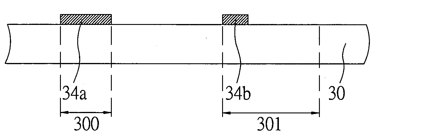
[0033]As shown in FIG. 3A, the method comprises providing at least one circuit board 30, wherein a surface of the circuit board 30 is defined with a first predetermined area 300 and a second predetermined area 301 for forming an electrically connecting pad.

[0034]As shown in FIG. 3B, the method further comprises: forming a resist 33 on the circuit board 30, wherein the resist 33 can be a photoresist, such as a dry film photoresist and a liquid photoresist, formed on the circuit board 30 by stencil printing, spin...


PUM


Abstract

An electrically connecting terminal structure of a circuit board and a manufacturing method thereof are disclosed. The method includes: providing a circuit board defined with first and second predetermined areas; forming the first electrically connecting pad in the first predetermined area and the second electrically connecting pad in a portion of the second predetermined area; forming an insulated protecting layer on the circuit board, forming openings on the insulated protecting layer for exposing the first and second electrically connecting pads and a pad-uncovered portion of the second predetermined area; forming a conductive layer on the insulated protecting layer and forming openings of the insulated protecting layer; forming a resist on the conductive layer, forming openings on the resist above the openings of the insulated protecting layer; and forming first and second metals in the openings above the first and second electrically connecting pads and the pad-uncovered portion of the second predetermined area.

Description

BACKGROUND OF THE INVENTION[0001]1. Field of the Invention[0002]The present invention relates to electrically connecting terminal structures for a circuit board and a manufacturing method of the structures, and more particularly, to a method for manufacturing an electrically connecting terminal structure of a circuit board by electroplating.[0003]2. Description of the Prior Art[0004]Flip chip package technology was introduced into the industry by IBM in the early 1960s. Unlike wire bonding technology, flip chip package technology involves implementing electrical connection between a semiconductor chip and a circuit board by solder bumps instead of gold wires. Flip chip package technology spares the use of long gold wires and thereby enables reduction of impedance. In view of this, the technique of applying high-temperature solder to a ceramic substrate, or control collapse chip connection (i.e., “C4”), has been in use for years. Recent years saw an increasing demand for high-density...

Claims


Application Information

Patent Timeline
IPC IPC(8): H05K1/00
CPCH05K3/244H05K3/3473H05K2201/094H05K2203/054H05K2201/09563H05K2201/0989H05K2203/043H05K2201/09436
Inventor SHIH, CHAO-WEN
Owner PHOENIX PRECISION TECH CORP
Why Eureka
Try Eureka