Semiconductor device

a semiconductor device and semiconductor technology, applied in semiconductor devices, instruments, computing, etc., can solve problems such as easy breakage of ic tags, and achieve the effects of preventing the malfunction of integrated circuits due to stress, improving stiffness of semiconductor devices, and reducing the risk of bending stress

Active Publication Date: 2008-01-31
SEMICON ENERGY LAB CO LTD
View PDF58 Cites 19 Cited by
  • Summary
  • Abstract
  • Description
  • Claims
  • Application Information

AI Technical Summary

Benefits of technology

[0013]According to the present invention, when the structural body formed of ceramics or the like is used, stiffness of the semiconductor device can be improved. Accordingly, even when an IC tag or the semiconductor device having the equivalent function is thinned, their required functions and robustness can be maintained. For example, even when pressing pressure is applied by a pointed object such as a pen tip, malfunction of an integrated circuit due to stress can be prevented. Moreover, resistance to bending stress can also be provided. In addition, when a wiring for connection is formed in the structural body formed of ceramics or the like in order to connect an antenna and the integrated circuit, malfunction caused by detachment of a connection portion can be prevented even when bending stress is applied.

Problems solved by technology

However, there arises a problem such that an IC tag is easily broken by pressing pressure or bending stress applied by a pointed object, as the IC tag becomes thin.

Method used


Image

  • Semiconductor device
  • Semiconductor device
  • Semiconductor device

Examples


embodiment 1

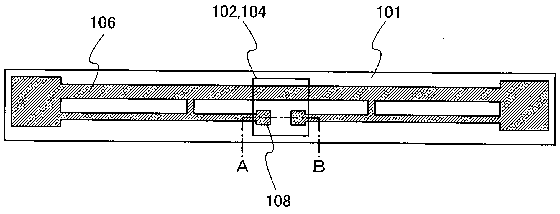
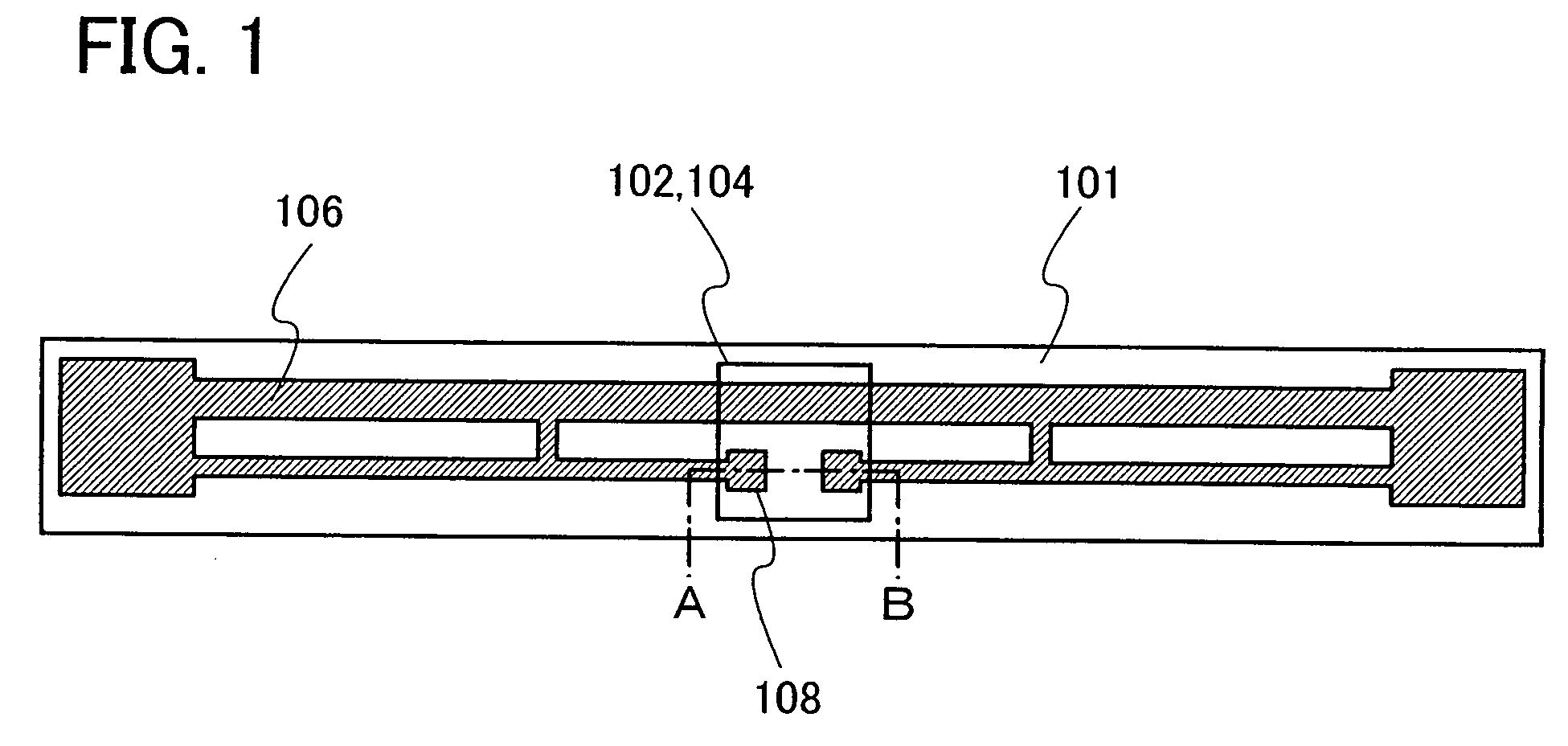
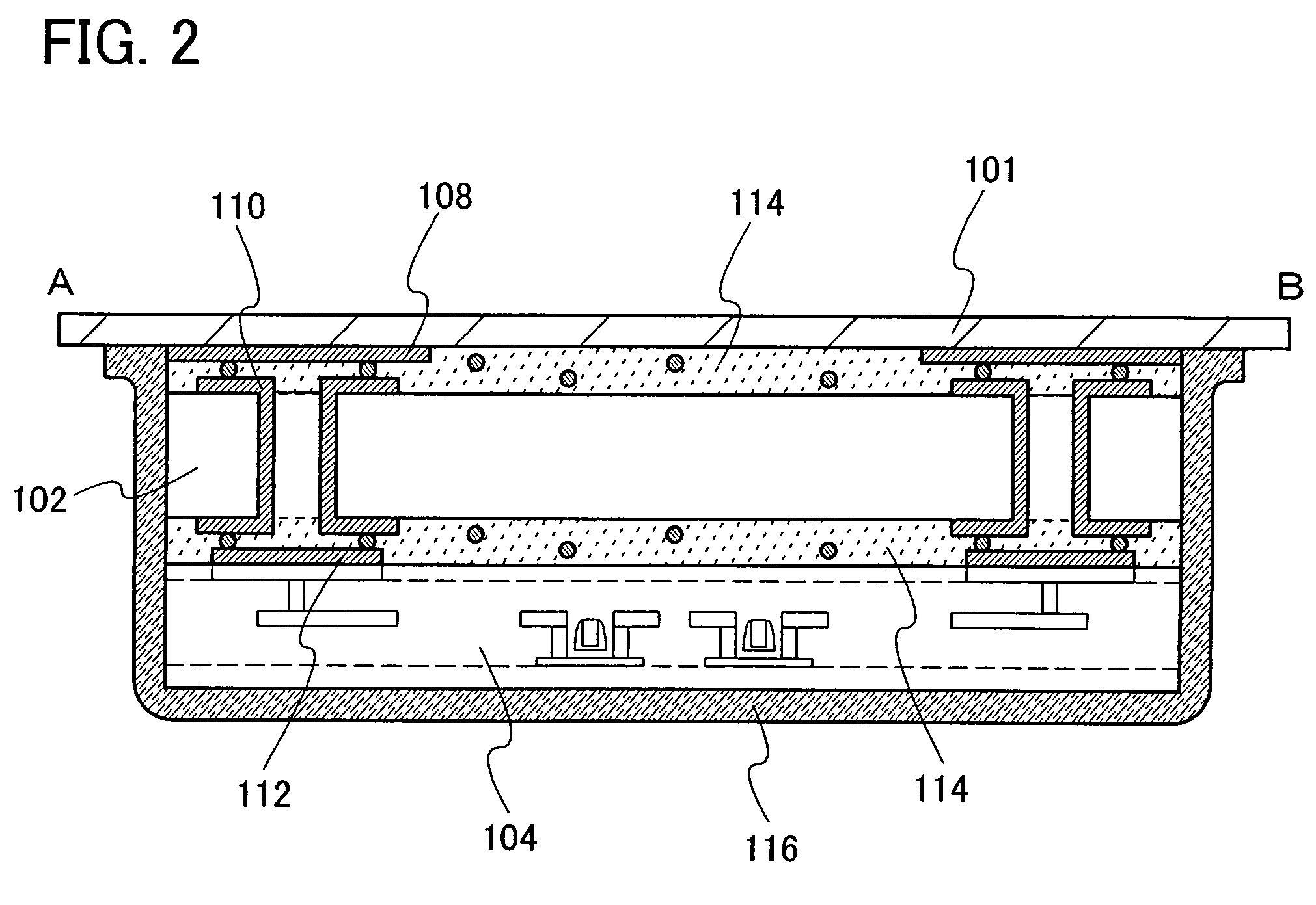
[0049]In this embodiment, one example of a semiconductor device in which a first structural body provided with an antenna, a second structural body provided with a capacitor portion, and an integrated circuit are combined is described with reference to FIGS. 5A to 6B. Note that FIGS. 5A to 5C are plan views showing the semiconductor device, and FIGS. 6A and 6B are cross-sectional views taken along lines A-B and C-D, respectively.

[0050]FIG. 5A shows a mode in which the antenna 106 having a coil-shape is formed in the first structural body 101. The first structural body 101 is formed of a plastic material such as PET (poly ethylene terephthalate), PEN (polyethylene naphthalate), PES (polyethersulfone), polypropylene, polypropylene sulfide, polycarbonate, polyether imide, polyphenylene sulfide, polyphenylene oxide, polysulfone, polyphthalamide, acrylic, or polyimide, or an insulating material such as nonwoven fabric or paper.

[0051]The antenna 106 is formed using a low resistant metal m...

embodiment 2

[0059]In this embodiment, one example of a semiconductor device including a first structural body provided with an antenna, a second structural body provided with a capacitor portion, an integrated circuit, and a ceramic antenna 122 is described with reference to FIGS. 7A to 8B. Note that FIGS. 7A to 7C are plan views showing the semiconductor device, and FIGS. 8A and 8B are cross-sectional views taken along lines E-F and G-H, respectively.

[0060]In FIG. 7A, the antenna 106 having a coil-shape is formed in the first structural body 101. The shape of the antenna 106 may be appropriately set in accordance with a wavelength which is used for communication, as in Embodiment 1.

[0061]FIG. 7A shows a structure in which the second structural body 102, the integrated circuit 104, and the ceramic antenna 122 are provided in accordance with the antenna terminal 108. FIG. 7B shows a plan view of the second structural body 102, FIG. 7C shows a plan view of the integrated circuit 104, and FIG. 7D ...

embodiment 3

[0067]In this embodiment, an example of a semiconductor device which includes a booster coil in order to increase a communication distance is described with reference to FIGS. 9A to 10B. A semiconductor device of this embodiment has an integrated circuit provided with a first antenna, a second structural body provided with a second antenna which is electromagnetically coupled with the first antenna, and a first structural body provided with a third antenna which is electromagnetically coupled with a reader / writer. Note that FIGS. 9A to 9C are plan views showing the semiconductor device, and FIGS. 10A and 10B are cross-sectional views taken along lines J-K and L-M, respectively.

[0068]In FIG. 9A, a third antenna 105 which is electromagnetically coupled with a reader / writer is formed in the first structural body 101. The third antenna 105 is formed, as in Embodiment 1.

[0069]The second structural body 102 and the integrated circuit 104 are provided in accordance with the antenna termina...


PUM


Abstract

When letters are written with a ballpoint pen, pen pressure is greater than or equal to 10 MPa. The IC tag embedded in the paper base material is required to withstand such pen pressure. An integrated circuit including a functional circuit which transmits and receive, performs arithmetic of, and stores information is thinned, and also, when the integrated circuit and a structural body provided with an antenna or a wiring are attached, a second structural body formed of ceramics or the like is also attached to at the same time. When the second structural body formed of ceramics or the like is used, resistance to pressing pressure or bending stress applied externally can be realized. Further, a part of passive elements included in the integrated circuit can be transferred to the second structural body, which leads to reduction in area of the semiconductor device.

Description

BACKGROUND OF THE INVENTION[0001]1. Field of the Invention[0002]The present invention relates to an information recording carrier which is used for information technology referred to as RFID (Radio Frequency Identification). Specifically, the present invention relates to a semiconductor device capable of transmitting and receiving information via electromagnetic waves, which is also referred to as an IC tag.[0003]2. Description of the Related Art[0004]Information technology which is referred to as RFID (Radio Frequency Identification) has been spread. For example, an IC tag which is a tag with its outside dimension of several centimeters and which stores data communicates with a reader wirelessly is known. An IC tag includes an antenna and an IC chip having a communication circuit and a memory.[0005]As one mode of an IC tag, a mode in which an antenna and an IC chip are embedded in paper is known. For example, a mode in which, in order to embed an IC tag having a thickness of less t...

Claims


Application Information

Patent Timeline
Patent Type & Authority Applications(United States)
IPC IPC(8): H01L29/00
CPCG06K19/07749
Inventor YAMAZAKI, SHUNPEIARAI, YASUYUKI
Owner SEMICON ENERGY LAB CO LTD
Why Eureka
Try Eureka