
Eureka
For R&D, Eureka makes reading and utilizing patents & technical documents easy.
Eureka AIR
Designed for self-driven R&D workflows. Generate viable solutions, solve complex R&D challenges, empower your innovation with AI.

Eureka Materials
Designed for material experts only. Revolutionize your material R&D, from search, analyze, to developing new materials.

TechResearch
Generate reliable direction feasibility study reports for your R&D in just a few steps.

TechSeek
Discover and master advanced knowledge NOW. Basics, ideas, possibilities, all at once.

TechMind
As an expert in R&D Theories, TechMind can generates customized viable solutions instantly.

TechRisk
Analyze your overall solution with one click, know your potential R&D risks in advance.

TechMonitor
Get weekly tech updates, stay abreast of the latest tech innovations and key insights.
Optical sensor and solid-state imaging device
- Summary
- Abstract
- Description
- Claims
- Application Information
AI Technical Summary
Benefits of technology
Problems solved by technology
Method used
Image

Examples
first embodiment
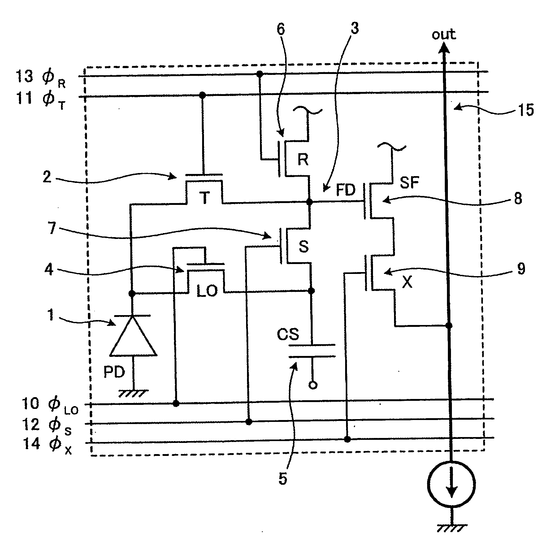
[0075]FIG. 6 shows an equivalent circuit of a pixel in the solid-state imaging device according to a first embodiment of the present invention, and FIG. 7 is a schematic plan view thereof.
[0076]Each pixel comprises: a photodiode PD1 that receives light and that produces and stores photocharges; a transfer transistor T2 provided adjacently to the photodiode PD1 and transferring the photocharges; a floating region (floating region) FD3 connected to the photodiode PD1 via the transfer transistor T2; an overflow gate LO4 provided adjacently to the photodiode PD1 and transferring photocharges that overflow the photodiode PD1 during a storage operation; a storage capacitor CS5 that stores photocharges overflowing the photodiode PD1 through the overflow gate LO4 during the storage operation; a reset transistor R6 connected to the floating region FD3, for discharging signal charges in the storage capacitor CS5 and the floating region FD3; a storage transistor S7 provided between the floatin...
second embodiment
[0107]The solid-state imaging device according to this embodiment is one in which the circuit configuration of the pixel in the solid-state imaging device according to the first embodiment is modified. FIG. 11 is an equivalent circuit digram of one pixel in this embodiment, and FIG. 12 is a schematic plan view thereof.
[0108]Each pixel comprises: a photodiode PD1 that receives light and that produces and stores photocharges; a transfer transistor T2 provided adjacently to the photodiode PD1 and transferring the photocharges; a floating region FD3 connected to the photodiode PD1 via the transfer transistor T2; an overflow gate LO4 provided adjacently to the photodiode PD1 and transferring photocharges that overflow the photodiode PD1 during a storage operation; a storage capacitor CS5 that stores photocharges overflowing the photodiode PD1 through the overflow gate LO4 during the storage operation; a reset transistor R6 connected to the storage capacitor CS5, for discharging signal ch...
third embodiment
[0121]The solid-state imaging device according to this embodiment is one in which the overflow gates of the pixels in the solid-state imaging device according to the first and second embodiments of the present invention are modified. FIGS. 14 and 15, respectively, are an equivalent circuit diagram and schematic plan view of a pixel in this embodiment, these figures corresponding to the respective figures of the first embodiment. Also, FIGS. 16 and 17, respectively, are an equivalent circuit diagram and schematic plan view of a pixel in this embodiment, these figures corresponding to the respective figures of the second embodiment.
[0122]Each pixel comprises: a photodiode PD1 that receives light and that produces and stores photocharges; a transfer transistor T2 provided adjacently to the photodiode PD1 and transferring the photocharges; a floating region FD3 connected to the photodiode PD1 via the transfer transistor T2; an overflow gate LO4′ provided adjacently to the photodiode PD1...
PUM
 Abstract
Description
Claims
Application Information
 - R&D Engineer
- R&D Manager
- IP Professional
- Industry Leading Data Capabilities
- Powerful AI technology
- Patent DNA Extraction
Browse by: Latest US Patents, China's latest patents, Technical Efficacy Thesaurus, Application Domain, Technology Topic, Popular Technical Reports.
© 2024 PatSnap. All rights reserved.Legal|Privacy policy|Modern Slavery Act Transparency Statement|Sitemap|About US| Contact US: help@patsnap.com