Photoelectric conversion apparatus, control method thereof, imaging apparatus, and imaging system

a technology of photoelectric conversion apparatus and control method, which is applied in the direction of television system, television system scanning details, radioation controlled devices, etc., can solve the problems of image quality degradation, blackening, and image quality degradation, so as to prevent the degradation of image quality of the photoelectric conversion apparatus and improve the subthreshold characteristics

Active Publication Date: 2008-02-14
CANON KK
View PDF16 Cites 68 Cited by
  • Summary
  • Abstract
  • Description
  • Claims
  • Application Information

AI Technical Summary

Benefits of technology

[0011]The present invention is provided to prevent degradation in image quality of a photoelectric conversion apparatus due to reception of light from a strong light source effectively, thereby improving the subthreshold characteristics in such cases.

Problems solved by technology

Additionally, blackening may take place; a part which has been struck by a particularly strong light component of the spotlight blackens.
For this reason, even when strong light is uniformly incident on the screen, the pixel exhibits a low-luminance output such as gray, resulting in degradation in image quality.
This considerably degrades the image quality; the luminance on the whole screen suffers graininess.
However, if they have a large electric potential difference, and the clip level is low, it is unlikely that a decrease in reset level upon incidence of strong light is detected.
However, if these potentials are close to each other, the reset level and set clip potential may reverse due to, for example, manufacturing variations, resulting in blackening.

Method used


Image

  • Photoelectric conversion apparatus, control method thereof, imaging apparatus, and imaging system
  • Photoelectric conversion apparatus, control method thereof, imaging apparatus, and imaging system
  • Photoelectric conversion apparatus, control method thereof, imaging apparatus, and imaging system

Examples


first embodiment

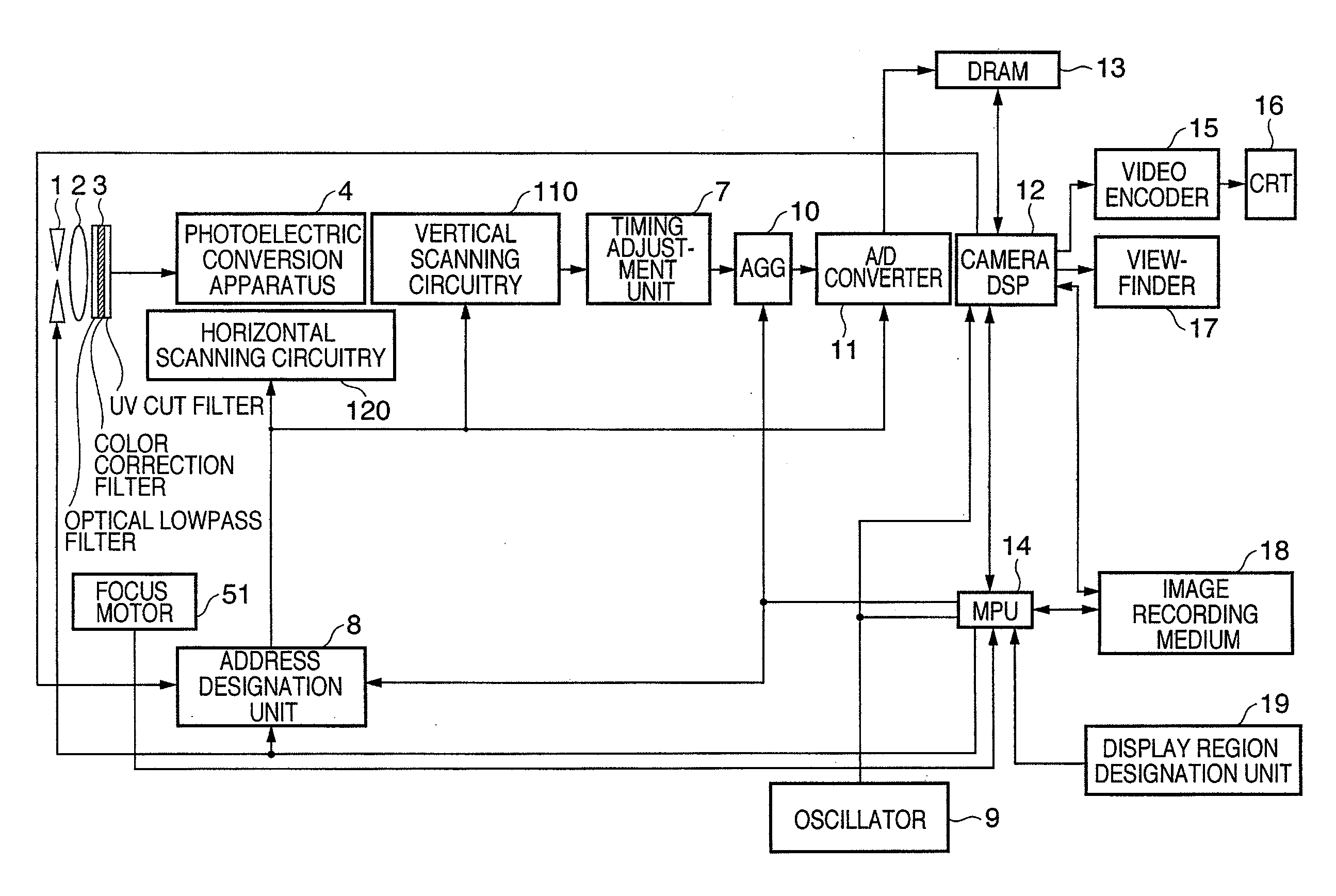
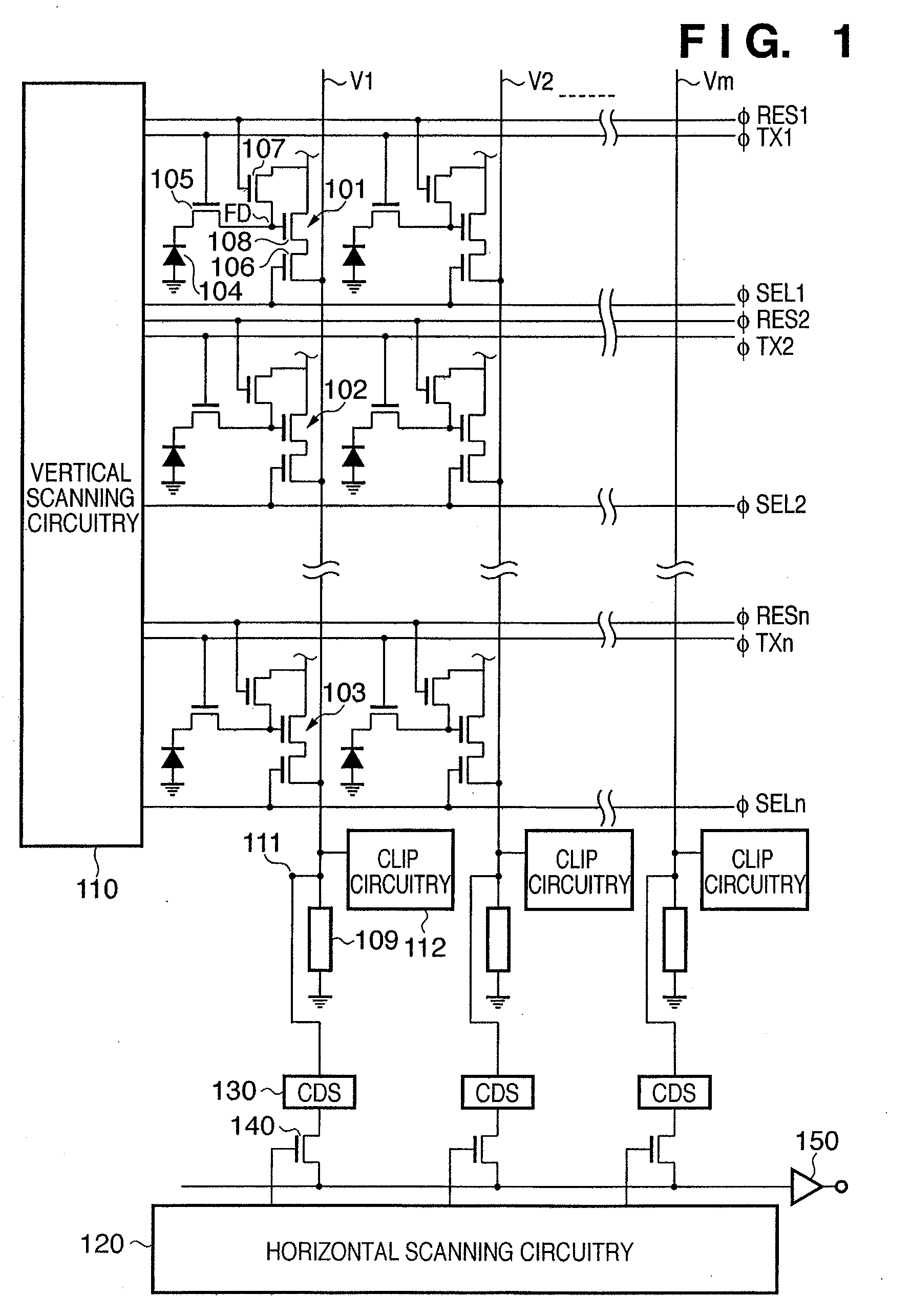
[0027]FIG. 1 is a view showing the arrangement of an imaging apparatus according to the first preferred embodiment of the present invention. The imaging apparatus includes a plurality of pixels 101 to 103. For illustrative convenience, FIG. 1 shows pixels of 3 rows×2 columns. However, the present invention is not limited to this, and it is possible to array an arbitrary number of pixels in the row and column directions. Each of the pixels 101 to 103 includes a photodiode 104 serving as a photoelectric conversion element, a transfer transistor 105, a floating diffusion FD, a selection transistor 106, a reset switch 107, and a source follower transistor 108. The imaging apparatus also includes vertical output lines V1 to Vm (m is an integer: m≧2, and the same will apply hereinafter), current source loads 109 serving as the load of the source follower transistors 108, selector switches 140, an output amplifier 150, vertical scanning circuitry 110, CDS circuitry 130, and horizontal scan...

second embodiment

[0044]FIG. 4 is a view showing an arrangement of an imaging apparatus according to the second preferred embodiment of the present invention. The imaging apparatus includes a plurality of pixels 101 to 103, as in the first embodiment.

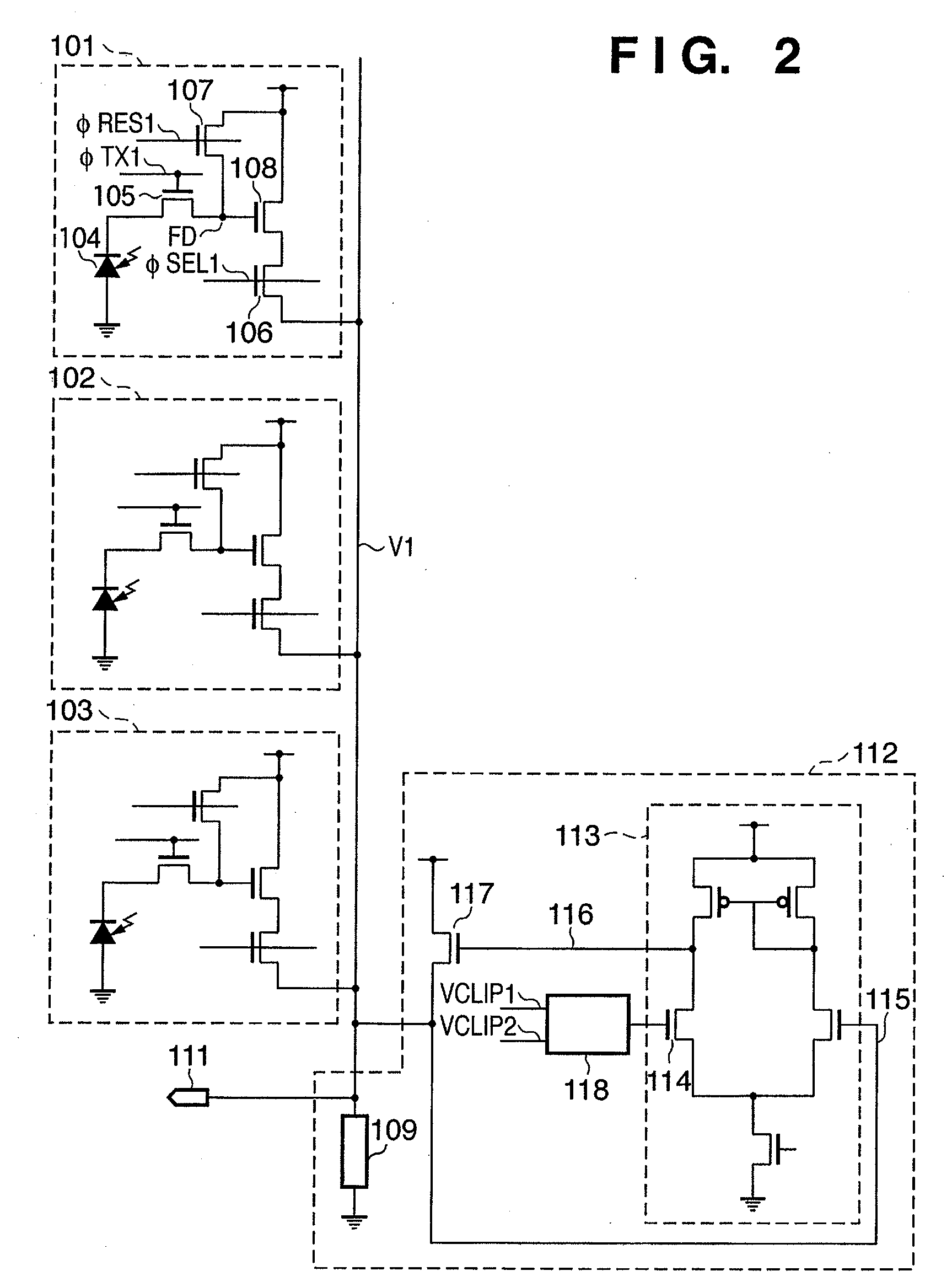
[0045]Clip circuitry 112 has amplifying circuitry including a common gate amplifier 163 and a common source amplifier 164. The common gate amplifier 163 outputs a voltage according to the difference between a vertical output line V1 and VCLIP1 to a node 167. The common source amplifier 164 has the node 167 as an input node. The common source amplifier 164 and the source followers of the pixels 101 to 103 share a current source load 109. The output node of the common source amplifier 164 connects to vertical output line V1.

[0046]The operation of the imaging apparatus according to this embodiment will be described next. The operation of the first embodiment can directly apply to the operation timing of a pixel of the imaging apparatus according to this emb...

third embodiment

[0052]In the third preferred embodiment of the present invention, an embodiment that controls the clip operation by controlling, for each column, the value of the current to flow to the current source load of a common gate amplifier 163 in the clip circuitry of the second embodiment will be described. This embodiment allows to improve the signal nonuniformity between columns, which takes place due to characteristic variations between clip circuitry by manufacturing variations.

[0053]FIG. 5 is a view showing an arrangement of an imaging apparatus according to the third preferred embodiment of the present invention. A D / A (Digital to Analog) converter 210 that supplies a bias voltage to the current source load of a common gate amplifier connects to each clip circuitry 112. A column memory unit 220 connects to the D / A converter 210. An external input terminal 240 connects to each column memory unit 220 via a column memory selector switch 230.

[0054]The operation of the imaging apparatus ...


PUM


Abstract

Each pixel has a photoelectric conversion unit configured to convert light into electrical charges and to store the electrical charges, an amplifying unit configured to amplify a signal based on the electrical charges stored in the photoelectric conversion unit and to output the signal to an output line, and a reset unit configured to reset a input part of the amplifying unit. A clip unit, which is configured to limit an electric voltage of the output line, includes an amplifying circuitry for amplifying a signal based on the electric voltage of the output line and an MOS transistor for limiting the electric voltage of the output line based on the difference in electric potential between the gate and source. The clip unit controls the electric potential of the gate of the MOS transistor by the amplifying circuitry.

Description

BACKGROUND OF THE INVENTION[0001]1. Field of the Invention[0002]The present invention generally relates to a method and apparatus for preventing degradation in image quality of a photoelectric conversion apparatus due to reception of light from a strong light source.[0003]2. Description of the Related Art[0004]An imaging apparatus such as a digital camera generally includes a photographing optical system and a photoelectric conversion apparatus that photoelectrically converts an object image formed by the photographing optical system. Photoelectric conversion apparatuses can be divided into either passive pixel sensors (PPS) or active pixel sensors (APS). PPSs are non-amplification sensors whose pixels have no function of amplifying electrical charges. PPSs include, for example, a CCD image sensor. APSs are amplification sensors whose pixels have a function of amplifying electrical charges. APSs include, for example, a CMOS image sensor. A CCD image sensor is advantageous for miniat...

Claims


Application Information

Patent Timeline
Patent Type & Authority Applications(United States)
IPC IPC(8): H04N5/335H01L27/146H04N5/357H04N5/369H04N5/374H04N5/3745H04N5/378
CPCH04N5/3598H04N25/627
Inventor YAMASHITA, YUICHIROKATO, SATOSHIONO, TOSHIAKITAKAHASHI, HIDEKAZU
Owner CANON KK
Why Eureka
Try Eureka