Liquid Crystal Display Device

a liquid crystal display and thin film transistor technology, applied in non-linear optics, instruments, optics, etc., can solve problems such as inconvenient repair of transistors, black spot defects, and bright spot defects, and achieve the effect of easy repair and maintenan

Active Publication Date: 2008-02-14
JAPAN DISPLAY INC +1
View PDF5 Cites 5 Cited by
  • Summary
  • Abstract
  • Description
  • Claims
  • Application Information

AI Technical Summary

Benefits of technology

[0016] In the present invention, a spare transistor not connected to a data signal line and a pixel electrode is formed in addition to a normal transistor for driving a pixel. Then, at the stage when an abnormality has been discovered in the operation of the normal transistor for driving the pixel, this transistor is cut off from the data signal line and the pixel electrode, and the spare transistor is connected to the data signal line and the pixel electrode.

Problems solved by technology

When an operation abnormality occurs in these transistors, a bright spot defect or a black spot defect occurs depending on the relationship between the content of the abnormality and the operation mode of the liquid crystal.
There are various methods for repairing these defects, but it is difficult to repair a transistor whose operation has become abnormal, and black spot repair that abandons drive operation resulting from a transistor and wires a pixel electrode to another line and a method that wires a pixel electrode to another pixel electrode to perform the same display with two pixels and make the defect inconspicuous are common.
Further, the method of cutting off a pixel connected to an operationally abnormal transistor from the operationally abnormal pixel and connecting the pixel to an adjacent pixel is effective when displaying white, but when red, green, and blue are displayed using a color filter of a single color, a phenomenon occurs where a pixel that is not supposed to light up ends up lighting up or a pixel that is supposed to light up ends up not lighting up, so it is difficult to say that the repair is infallible.
Moreover, the method of connecting two transistors to one pixel cannot be employed in large-screen high-definition products because parasitic capacitance between the gate lines and the data lines becomes large, the problem of signal delay occurs, and the brightness within the screen becomes non-uniform.

Method used


Image

  • Liquid Crystal Display Device
  • Liquid Crystal Display Device
  • Liquid Crystal Display Device

Examples


third embodiment

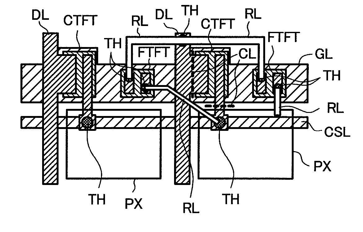
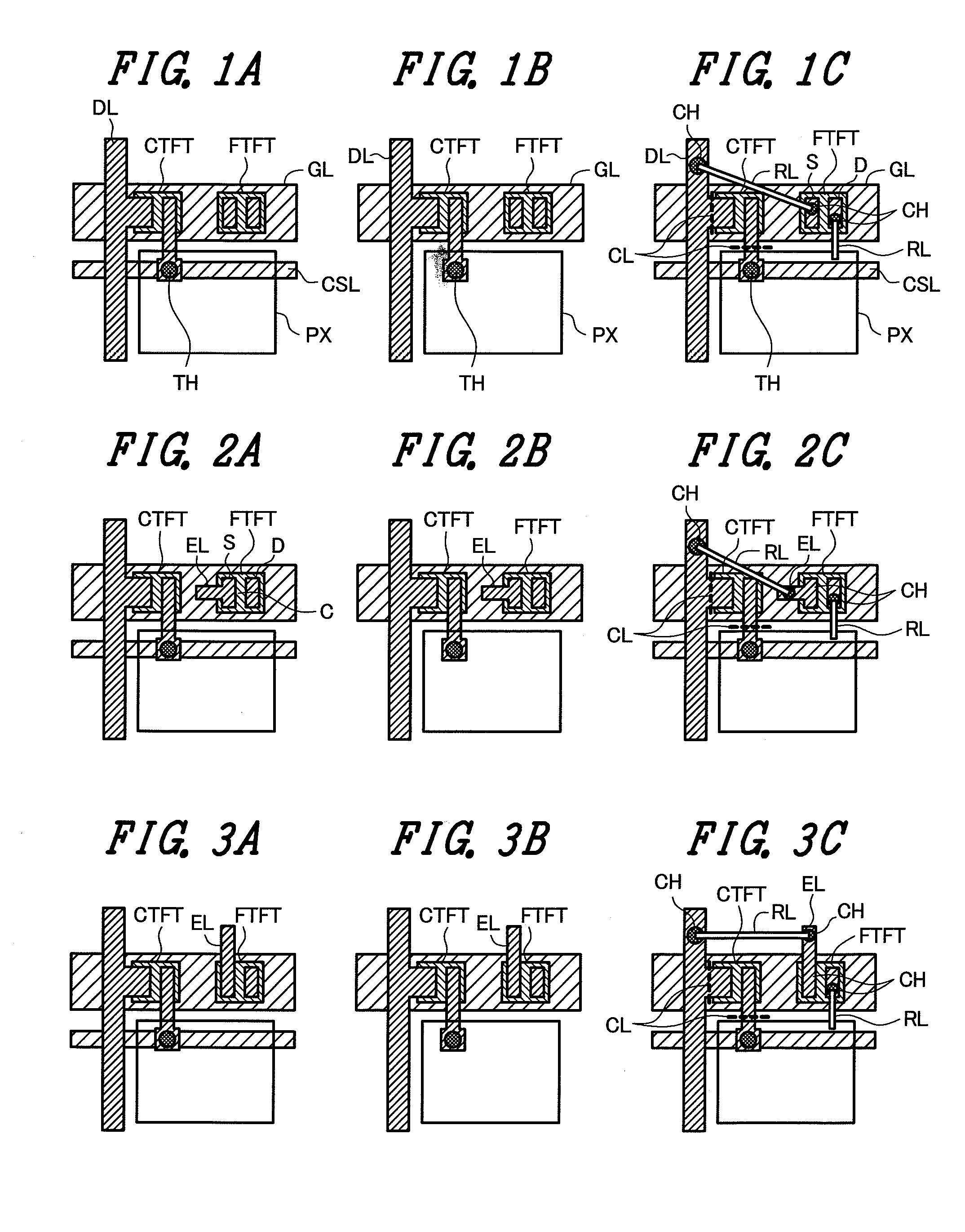
[0052]FIGS. 3A to 3C are configural diagrams of the pixel portion of the present embodiment. What is different from the second embodiment shown in FIGS. 2A to 2C is that the leader line EL for repair connection is led out as far as the outside of the gate line GL. FIGS. 3A, 3B, and 3C correspond to FIGS. 2A, 2B, and 2C, and description of the same reference letters will be omitted.

[0053] Turning now to FIGS. 3A to 3C, a heat process such as laser CVD is used in the formation of the contact holes CH and in the connection of the repair lines RL when the spare transistor FTFT is to be connected to the data signal line DL and the pixel electrode PX. For that reason, when the leader line EL is disposed on the gate line GL and the contact hole CH is formed as in the second embodiment, there is the potential for the insulating film between the leader line EL and the gate line GL to be destroyed by heat. Thus, in the present embodiment, the leader line is led out as far as the outside of t...

fourth embodiment

[0055]FIGS. 4A to 4C are configural diagrams of the pixel portion of the present embodiment. What is different from the second and third embodiments shown in FIGS. 2A to 2C and FIGS. 3A to 3C is that it is ensured that leader lines EL do not intersect the pixel electrode PX and the holding capacity line CSL. FIGS. 4A, 4B, and 4C correspond to FIGS. 2A, 2B, 2C and FIGS. 3A, 3B, and 3C, and description of the same reference letters will be omitted.

[0056] Turning now to FIGS. 4A to 4C, when a leader line EL from the drain electrode D of the spare transistor FTFT planarly intersects the pixel electrode PX, parasitic capacitance between the pixel electrode PX (or the drain electrode D) and the gate line GL becomes larger, which causes a problem in the uniformity of display within the screen. Thus, in the present embodiment, when the leader line EL is formed in the direction of the pixel electrode PX, the leader line EL does not planarly intersect the pixel electrode PX. Similarly, the l...

fifth embodiment

[0057]FIGS. 5A to 5C are configural diagrams of the pixel portion of the present embodiment. What is different from the embodiments heretofore is that the leader lines EL from the spare transistor FTFT planarly intersect both the data line DL and the pixel electrode PX, but they are placed in a floating state where they are not connected in terms of direct current. FIGS. 5A, 5B, and 5C correspond to A, B, and C of the heretofore figures, and description of the same reference letters will be omitted.

[0058] Turning now to FIGS. 5A to 5C, a floating metal FM is in the same layer as the gate line GL and planarly intersects the data signal line DL via an insulating layer. The leader line EL from the spare transistor FTFT and the data signal line DL are in the same layer and overlap the floating metal FM via the insulating film. As shown in FIG. 5C, this overlapping portion is capable of being connected by laser spots LS that have been heat-welded utilizing a laser or the like, so that c...


PUM

PropertyMeasurementUnit
angleaaaaaaaaaa
angleaaaaaaaaaa
angleaaaaaaaaaa

Abstract

A normal transistor CTFT connected to a data signal line DL and a pixel electrode PX and a spare transistor FTFT in a floating state are formed on a gate line GL. When an operational abnormality occurs in the normal transistor CTFT, the normal transistor CTFT is cut off from the data signal line DL and is cut off from the pixel electrode PX connected via a through hole TH by cutting lines CL. Thereafter, the spare transistor FTFT is connected to the data signal line DL and the pixel electrode PX by repair lines RL.

Description

CLAIM OF PRIORITY [0001] The present application claims priority from Japanese application serial No. 2006-118227, filed on (Apr. 21, 2006), the content of which is hereby incorporated by reference into this application. BACKGROUND OF THE INVENTION [0002] 1. Field of the Invention [0003] The present invention relates to a thin-film transistor liquid crystal display device, and deals with abnormality in the operation of a thin-film transistor. [0004] 2. Description of the Related Art [0005] A liquid crystal display element comprises a liquid crystal material interposed between two substrates that have been oriented, with the peripheral edges being sealed by a seal. The liquid crystal display element performs display as a result of the state of orientation of the liquid crystal material interposed between the two substrates being controlled. The techniques for controlling this state of orientation are various, but a technique is widely and commonly performed where the state of orienta...

Claims


Application Information

Patent Timeline
Patent Type & Authority Applications(United States)
IPC IPC(8): G02F1/1333
CPCG02F1/13624G02F2001/136268G02F1/136259G02F1/136268
Inventor KAWAMURA, TETSUYASATO, MASASHIOOKAWA, MASANORIKAMOSHIDA, KENTAKURAHASHI, NAGATOSHIIWATO, HIROAKI
Owner JAPAN DISPLAY INC
Why Eureka
Try Eureka