Device manufacturing method and device, electro-optic device, and electronic equipment

a manufacturing method and device technology, applied in the direction of optics, transistors, instruments, etc., can solve the problems of low effective area utilization ratio of transistor circuits on the substrate of liquid crystal electro-optic devices, high manufacturing cost per unit area, and high cost. , to achieve the effect of low cost, effective manufacturing, and increased product yield ra

Active Publication Date: 2005-12-22
SAMSUNG ELECTRONICS CO LTD
View PDF4 Cites 8 Cited by
  • Summary
  • Abstract
  • Description
  • Claims
  • Application Information

AI Technical Summary

Benefits of technology

[0058] According to this electronic equipment, the device is manufactured effectively at low cost and product yield rate is also increased, so that the electronic equipment itself is also manufactured at low cost.
[0059] As described above, according to the manufacturing method for a device of the present invention, plural elements which are to be dispersingly arranged at intervals on the final substrate are concentratedly manufactured on the original substrate. Therefore, devices can be manufactured effectively at low cost.
[0060] Moreover, the plural elements which are concentratedly manufactured on the original substrate can be easily selected and removed before the transfer. As a result, product yield rate can be increased.
[0061] Furthermore, since the surface where the terminal sections of the elements are exposed is adhered via the conductive adhesive to the final substrate, then for example, by directly adhering the conductive adhesive to the conductive sections on the final substrate, adhesion of the elements to the final substrate and conducting the terminal sections with the conductive sections can be performed at the same time. Hence, the process for conducting the terminal sections with the conductive sections by wiring after transferring is obviated, enabling simplification of the processes and an increase in productivity.
[0062] Moreover, an element having a laminated structure which is conventionally difficult to manufacture can be provided, and an element having a three-dimensional structure can be easily manufactured.

Problems solved by technology

However, regarding the conventional electro-optic devices furnished with amorphous silicon TFT or polycrystalline silicon TFT, manufacturing cost per unit area is expensive.
Hence, in the case where large electro-optic devices are to be manufactured, a problem is that the cost becomes very expensive.
One cause for this is the effective area utilization ratio of the transistor circuit on the substrate of the liquid crystal electro-optic device is low, and wastage of the thin film element constituent material which forms the film is considerable.
However, in the microstructure technique, there is the problem in that reliable arrangement of the microstructures on the substrate and accurate positioning are difficult.
Moreover, since the directions in which the microstructures are arranged are random, special circuits to cope with this must be provided for the microstructures, with the problem of incurring a cost increase.
However, this conventional technique is used for manufacturing color filters or the like for liquid crystal display elements, and other application possibilities have not been specified.
However, the conventional transfer techniques have the following problems.
However, in order to manufacture a substrate for which the arranged area of the TFTs is small with respect to the whole substrate area, it is necessary to specially manufacture a substrate where a large number of TFTs are formed at the same intervals as for the final substrate, and transfer these to the final substrate, or it is necessary to repeat the transfer many times, which does not always give a reduction in cost.
Further, since the conventional transfer techniques are to transfer all the thin film elements such as TFTs which are formed on the substrate onto the final substrate, then the larger the area of the substrate, the higher the characteristic required for the irradiating laser light, that is, the higher the power and uniformity, so that it becomes difficult to obtain a laser light source which satisfies the required performance, and large sized highly accurate irradiation equipment becomes necessary for the laser light irradiation.
In addition, when irradiating a high power laser light, the thin film elements may be heated above their heat resistant critical temperature, so that the function of the thin film element itself may be lost.
Hence, there is the problem that the transfer process itself becomes difficult.
Therefore cracking may occur when the final substrate is bent after the transfer, and the ability to follow the bending of the substrate is not good.
As a result, in the conventional transfer techniques, the degree of freedom for selecting the final substrate is limited.

Method used


Image

  • Device manufacturing method and device, electro-optic device, and electronic equipment
  • Device manufacturing method and device, electro-optic device, and electronic equipment
  • Device manufacturing method and device, electro-optic device, and electronic equipment

Examples


first embodiment

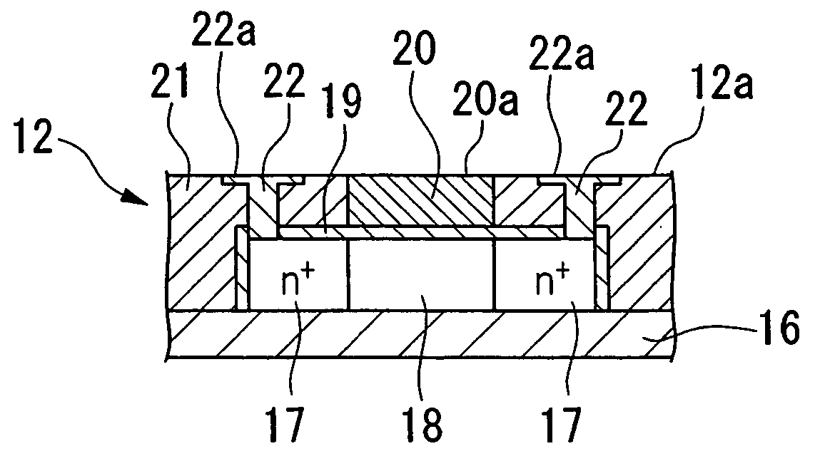
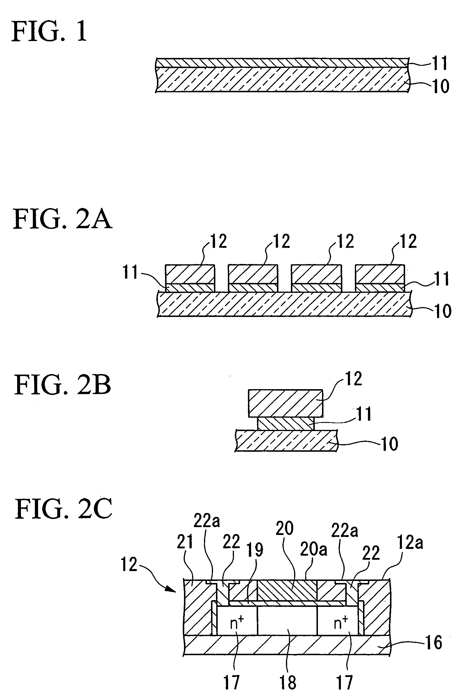
[0083]FIG. 1 to FIG. 7 are explanatory drawings of a first embodiment of the present invention (element transfer method). This element transfer method is an example of where an anisotropic conductive adhesive film is specifically used as a conductive adhesive, and is executed through the following first process to fourth process.

[0084] [First Process]

[0085] In the first process, as shown in FIG. 1, a separation layer 11 is formed on an original substrate 10, and furthermore, as shown in FIG. 2A, many elements 12 are formed on the separation layer 11.

[0086] The original substrate 10 in the present embodiment, is a substrate for element forming. Such an element forming substrate is preferably one having transmittance that allows transmission of light.

[0087] In this case, the transmissivity of light is preferably more than 10%, and more preferably more than 50%. If the transmissivity is too low, the loss of light becomes large, and a larger quantity of light is required in order to ...

second embodiment

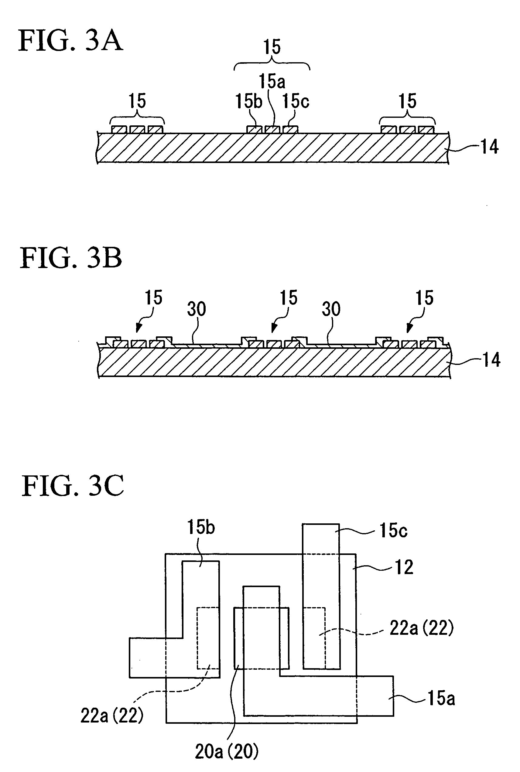
[0168] The difference of the second embodiment to the first embodiment is the point that anisotropic conductive adhesive in paste form, that is, in liquid form, is used as the conductive adhesive, instead of the film-like anisotropic conductive adhesive.

[0169] In this embodiment, the final substrate 14 shown in FIG. 3B formed with the wiring 30 for connecting to the electrode pads 15a, 15b, 15c is prepared, and liquid form anisotropic conductive adhesive 32 as shown in FIG. 10 is applied on this over the whole surface by spin coating.

[0170] The liquid form (paste form) anisotropic conductive adhesive 32 is not specifically limited, and various kinds can be used. Examples suitable for use include “3370G” made by Three Bond Co., Ltd. This anisotropic conductive adhesive 32, as with the film-like anisotropic conductive adhesive 32, is also formed by dispersing fine conductive particles in an insulative paste, and it is constituted so as to be cured by heat pressing.

[0171] After whol...

third embodiment

[0175] The difference of the third embodiment to the second embodiment is the point that the liquid form anisotropic conductive adhesive 32 is selectively arranged by a liquid droplet discharge method such as an inkjet method, a dispenser method, or the like, instead of whole surface application by spin coating.

[0176] In this embodiment, the final substrate 14 shown in FIG. 3B formed with the wiring 30 for connecting to the electrode pads 15a, 15b and 15c may be used. However, as shown in FIG. 11, the final substrate 14 formed with only the electrode pads 15a, 15b and 15c before forming the wiring 30 may also be used.

[0177] In the case where the final substrate formed with the only the electrode pads 15a, 15b and 15c is used, the anisotropic conductive adhesive 32 being in liquid form is discharged from a droplet discharge section, for example, an inkjet head H, so as not to cover the whole surface of these electrode pads 15a, 15b and 15c. Discharge of the anisotropic conductive a...


PUM

PropertyMeasurementUnit
temperatureaaaaaaaaaa
thicknessaaaaaaaaaa
thicknessaaaaaaaaaa

Abstract

A device manufacturing method, including: a first process for providing the plural elements on the original substrate via a separation layer in a condition where terminal sections are exposed to a surface on an opposite side to the separation layer; a second process for adhering the surface where the terminal sections of the elements to be transferred on the original substrate are exposed, via conductive adhesive, to a surface of the final substrate on a side where conductive sections for conducting with the terminal sections of the elements are provided; a third process for producing exfoliation in the separation layer between the original substrate and the final substrate; and a fourth process for separating the original substrate from which the transfer of elements has been completed, from the final substrate.

Description

[0001] This is a Division of application Ser. No. 10 / 756,416 filed Jan. 14, 2004. The entire disclosure of the prior application is hereby incorporated by reference herein in its entirety. Priority is claimed on Japanese Patent Application No. 2003-15097, filed Jan. 23, 2003, the content of which is incorporated herein by reference.BACKGROUND OF THE INVENTION [0002] The present invention relates to a manufacturing method for a device which manufactures a device by transferring elements, a device manufactured by the method, an electro-optic device, and electronic equipment. [0003] Recently, for electro-optic devices such as liquid crystal electro-optic devices, active matrix type devices which use thin film elements such as thin film transistors (hereunder, TFT), thin film diodes (hereunder, TFD) or the like, have become the mainstream. However, regarding the conventional electro-optic devices furnished with amorphous silicon TFT or polycrystalline silicon TFT, manufacturing cost per...

Claims


Application Information

Patent Timeline
Patent Type & Authority Applications(United States)
IPC IPC(8): G02F1/1368H01L21/02H01L21/336H01L21/77H01L21/84H01L27/108H01L27/12H01L27/13H01L29/745H01L29/786
CPCH01L27/1214H01L27/1266H01L2221/68363H01L29/78603H01L27/13H01L21/6835H01L2221/68322H01L2221/68381
Inventor HASHIMOTO, TAKASHITAKAKUWA, ATSUSHIKAMAKURA, TOMOYUKIUTSUNOMIYA, SUMIO
Owner SAMSUNG ELECTRONICS CO LTD
Why Eureka
Try Eureka